

Research report 1998
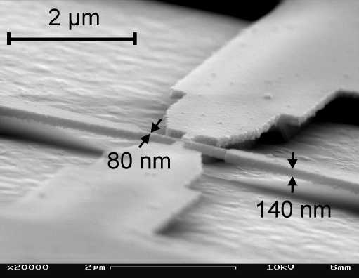
Figure 1. Free standing nanowire defined by high-resolution, low-energy
electron-beam lithography
Preface
This is our 5th web-based research report since we went 'online' in 1994. Since then, our website has attracted a lot of attention from all over the world and meanwhile serves as an information source not only for our physics colleagues and interested students but also for those out there, who simply want to know on which subjects their 'tax Euros' are working. We appreciate the tremendous activity on our server and do encourage everybody to come by and stay for a while!
For our group, the last year was an extremely sucessful one:
In total, the group published more than 35 scientific papers, and presented 15 invited talks on international conferences and workshops on various subjects and most importantly, 12 students finished their Diploma or PhD thesis. Dr. David Wharam accepted a professorship at the University of Tübingen - we wish him all the best! We had the pleasure to welcome a new member of our scientific staff, Dr. Robert Blick, who brought in new ideas and techniques, received the 'Walter-Schottky-Prize for Solid State Research', and finally, Jörg Kotthaus could be convinced to stay with us and hence to ensure the continuity of our daily work. Many visitors from abroad choose to spend some time with us or came by to give seminar talks.
Finally, we would like to encourage the readers of this (although somewhat delayed) report to contact us and to share their comments and ideas with us.....
Overview
Modern semiconductor technology nowadays combines more than ten million different transistors on a single chip barely as big as a thumbnail to form an extraordinary complex and sophisticated circuit. Following Moore's law, this very large scale integration will proceed over roughly the next ten years until a single element on a chip will be scaled down to less than about 50 nm. This typical dimension of a single device, however, represents a barrier, beyond which the basic operation of an electronic device starts to be based on fundamentally different mechanisms as compared to the conventional ones.
In a classical silicon MOSFET, for example, the principle of operation is based upon the statistical motion of about 10'000 electrons per square micron, whose number may be varied by an external electrode via electric fields. This movement takes place close to the relatively rough silicon/silicon dioxide interface and is described by diffusive processes, similar to the Brown's motion of molecules.
If, however, the dimension of a device becomes comparable or even smaller than the typical distance between two scattering events, the electrons start to move ballistically, like the balls on a billiard table. Moreover, at these small sizes, the number of electrons within a single device starts to approach one. For even smaller devices, their size becomes comparable to the wavelength of the electrons themselves - typically some ten nanometers in this case: The description of the electrons behaving like little charged spheres starts to fail and to require for a quantum mechanical formulation of the device.
In our group, we investigate the electronic, electrooptical, and electromechanical properties of specially tailored semiconductor structures with typical dimensions of the order or less than 100 nm. Recently, we also started to process and investigate mechanical systems like resonators and oscillators on the nanometer scale. Our goal is the detailed understanding of the new physical phenomena associated with a dramatic reduction of size, to explore new grounds for future device applications, and to be prepared for the day when nano-electronics will take over the role of micro-electronics and micro or nano-mechanics will open new routes to the tiny ultra small universe!
- to boldly go where no person has ever gone before !
The research in our group is based on three fundamental prerequisites:
- Nanotechnology
- Sophisticated electronic and optical experimental techniques
- Quantum mechanical concepts and analysis
Starting from suited semiconductor layered systems, we first have to prepare the desired structures with lateral nanometer size dimensions. We use and develop different nanotechnologies that enable us to scale down the size of our structures to the size of the electronic wavelength. For this purpose, our nanotechnology labs are located in a dust free cleanroom area containing modern semiconductor processing equipment.
As we're always trying to be internationally competitive, we set up a large number of international co-operations with partners being specialized in the epitaxial growth of our high quality starting material. Meanwhile, our nanotechnological techniques are also transferred to different disciplines of leading edge research resulting in newly developed collaborations with highly qualified specialists in x-ray analysis, polymer physics and biophysics.
Secondly, we constantly develop and apply sensitive experimental techniques which enable us to chararcterize and to investigate the electronic and optical properties of our nanometer scale samples over the whole spectral range starting from DC over the microwave and infrared regime, the visible spectrum up to UV. At the same time, we are equipped with facilities allowing fo extremely low temperatures and high magnetic fields - invaluable tools for the detailed understanding of the quantum mechanic phenomena in our devices.
A third prerequisite for our research is a detailed and fundamental theoretical analysis and understanding of nanophysics. Together with many theoretical groups and in a very fruitful atmosphere of collaboration, we try to develop new theories and techniques helping us to understand or to predict the many fascinating effects that we are constantly facing. This is in particular important, as we are not studying systems already existing in nature but try to artificially tailor small pieces of this nature to behave in a desired fashion.
A. Transport Properties
A.1. Interaction of Surface Acoustic Waves (SAW) and Low-Dimensional Electron Systems
Figure 2. Hybrid-based acoustic charge transport device operating at room temperature. The device consists of a thin GaAs/InGaAs semiconductor quantum layer containing a quantum well with a two-dimensional electron system that is transferred onto a strongly piezoelectric substrate. On this substrate, a surface wave is propagating. The interaction between the large amplitude wave and the electron system leads to new, nonlinear effects and to acoustic charge transport across the mm long sample.
Surface acoustic waves are modes of elastic energy which can propagate on the surface of different materials. If the substrate is piezoelectric, those waves are accompanied by electric fields which then propagate at the speed of sound. The electric fields of the wave can couple to the mobile carriers within a semiconductor structure and modify its electronic and elastic properties. By measuring the attenuation of the wave and the renormalization of the sound velocity we can, for instance, extract information on the dynamic conductivity of the electron system. We also investigate the possibility to use a SAW for a dynamical lateral potential modulation and we investigate the influence of a SAW onto the optical properties of an electron system. Our experiments presently cover the frequency range between 100 MHz and 6 GHz, corresponding to surface acoustic wavelengths between 30 mum and 500 nm, respectively.
The SAW - related research in 1998 was again governed by two different topics:
- Hybridization of piezoelectrics and semiconductors, exploring possible device applications and nonlinear effects
- Optical investigations of the SAW - semiconductor interaction
Our recent progress in fabricating high frequency and multi-frequency SAW transducers enables us to expand our SAW transport studies well into the GHz regime. The possibility to generate multiple frequencies on a single device allows for a detailed investigation of the SAW - 2DES interaction as a function of the frequency. On standard semiconductor heterojunctions, however, the strength of this interaction is rather weak. For this reason, we use hybrid structures consisting of a strong piezoelectric (LiNbO3) the active semiconductor layer structure. Here, a thin layer of the semiconductor structure containing the active heterojunction is removed from its substrate and tranferred onto a strongly piezoelectric host substrate.
The SAW - 2DES interaction can be enlarged by two orders of magnitude as compared to the monolithic case. This interaction is now strong enough to become technologically very attractive. Room temperature operation is also possible. Together with the Siemens research lab, we are presently developping new concepts for a technological exploitation of this approach. apart from technologically challenging projects, the hybridization technique also offers nice possibiliteis to explore the interaction between low-dimensional electron systems and surface acoustic waves with very large amplitudes. Here, we focussed on the investigation of nonlinear effects that arise under these conditions. For example, we could show that this nonlinear interaction leads to a strong decrease of the electronic absorption that is linked to a separation of a formally homogenous carrier density in the electronic system into well separated stripes riding the wave.
Our maior activities, however, concentrated on the investiagtion of the influence of a SAW on the optical properties of a semiconductor quantum well. Here, we opened a completely new and exciting area of research and attracted a tremendous national and international interest. We observe a strong influence of the SAW on the optical properties of a quantum well . The photoluminescence of the quantum well can be completely quenched under the influence of the SAW. Moreover, we show that the SAW can act as a "Photon Conveyor Belt", where optical signals can be stored by the SAW in the semiconductor and may be re-assembled into light after very long delay times and at a remote location of the sample!
Also, the possibility to deliberately pump a self-assembled quantum dot on the surface of a semiconductor quantum well has been investigated both experimentally as well as theoretically. In collaboration with the group of Prof. Fritz Haake (University of Essen), we have proposed a novel scheme for the generation of a single photon source using surface acoustic waves. A non-classical light might evolve from these studies, that we have also started to perform experimentally.
SAW-induced lateral potential modulations in hybrid systems could be shown to also act as an effective potential modulation for a quasi two-dimensional electron system under quantum conditions. For small wavelengths, we were able to observe commensurability oscillations in the acoustoelectric effect in such structures. Here, the classical cyclotron diameter equals the wavelength of the SAW, leading to pronounced oscillations in the acoustoelectric voltage across the semiconductor sample.
A.2. Electron Transport in Antidot-Lattices
"Antidot" lattices can be considered the complementary structure to quantum dot lattices: While in the latter, an array of isolated islands of electrons is created, in the former an array of small voids is cut out of a two-dimensional electron gas. In the past, a number of novel effects have been observed both in classical as well as quantum transport, which result from the interplay between different length scales in antidot-lattices (lattice period, magnetic length, Fermi-wavelength). Whereas commonly circular voids are patterned, we have created lattices of cross-shaped antidots. Such lateral superlattices can equally be regarded as antidot arrays, as two-dimensional arrays of quantum point contacts or as arrays of coupled quantum dots. They are therefore promising candidates to study the the transition between different types of quantization, e.g., between the quantized conduction in 1-dimensional channels at zero magnetic field and the quantum Hall effect in 2-dimensional electron gases at high fields. In the antidot picture, the complex unit cell is expected to lead to more complex carrier dynamics, compared to the well-investigated case of simple (round) antidots. Indeed, a number of novel structures in the magnetotransport properties of "+"-shaped antidots have been observed. Puzzling at first, the origin of these feature could be clarified by a detailed analysis of the quasi-classical ballistic electron trajectories, which was performed in collaboration with the Regensburg University.
A.3. Ballistic Rectifier
Furthermore, antidot lattices have been investigated where the triangular shape of the basis breaks the left-right symmetry of the electron system. In low frequency transport these samples exhibit maxima in the magnetotransport at a magnetic field where the cyclotron diameter equals half the lattice period. This is caused by so-called skipping orbits and shows that it is indeed possible to transfer triangular shapes with straight edges into the two-dimensional electron gas. In high-frequency experiments we observe lateral photo-voltages which closely reflect the features in low-frequency transport caused by the presence of the antidots. This might be due to the fact that the broken symmetry of the antidot-lattice leads to a rectification of the high-frequency radiation.
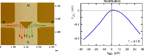
To further investigate the influence of symmetry-breaking on transport properties in mesoscopic semiconductor structures, we have fabricated cross junctions with an embedded triangular antidot. As seen in the figure, a simple picture of ballistic electron transport predicts unusual transport behaviour in such a device: Independent of current direction, electrons ejected out of the narrow channels (S and D) will be reflected from the edges of the antidot towards the lower (L) channel. This way, a voltage is induced between the L and the U channel which does NOT change sign, when the input current is reversed. Indeed, a clear voltage was observed experimentally on such samples, which exhibits the above mentioned unusual symmetry relations.
A.4. Coulomb Blockade Phenomena in Quantum Dots
If very small islands of electrons are isolated from a two-dimensional electron gas via tunnel barriers, the charging energy needed to add additional electrons to the island can be higher than the thermal energy available. In such a case, which usually requires very low temperatures, electron transport through such a 'quantum dot' is blocked.This so-called 'Coulomb blockade' can be raised by tuning the islandís energy with an additional plunger gate (see figure). A plunger gate sweep results in quasi-periodic conductance oscillations.
The difference between adjacent conductance maxima is the ëaddition energyí. In the simple ëconstant interactioní model this energy can be expressed as the sum of a classical capacitive charging term and a quantum-mechanical single particle energy level spacing.
We have performed Coulomb blockade measurements on a semiconductor quantum dot fabricated in a GaAs-AlGaAs-heterostructure and investigated the fluctuations and the distribution of the conductance peak spacings (9-97) obtained from these measurements. The statistical properties were compared to the predictions of random matrix theory (RMT) as this theory provides a very good description of the spectra of many complex systems.
It was found that the fluctuations in the peak spacings are larger than expected from RMT and the distribution of the spacings resembles a Gaussian rather than a Wigner-like probability distribution. This indicates that the peak spacings are strongly affected by the electronic interactions on the dot. However, both constant interaction model and RMT deal with single particle spectra. Until now, there is still put considerable theoretical effort on the understanding of the peak spacing distributions.
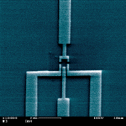
Figure 3. REM micrograph of an electrostatically defined quantum dot. Two tunnel contacts provide access to the transport properties of the dot, which can be controlled by using a central plunger gate. The lithograpically defined dot area is about 0.5 * 0.5 microns.
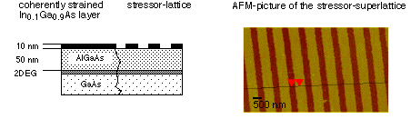
A.5. Epitaxial InGaAs surface stressors
With advances in miniaturization of semiconductor structures, the interplay between mechanical stress and electronic properties becomes more and more important. On the one hand, mechanical stress can limit the performance of small scale electronic devices. On the other hand, a controlled application of stress can be used to tailor the optical and electronic properties of semiconductor structures beyond common patterning techniques, such as etching or electrostatic modulation. We have used a novel type of a coherently strained stressor structure to create a one-dimensional periodic potential in the two-dimensional electron gas at a AlGaAs/ GaAs heterointerface. Contrary to conventional (e.g. evaporated or sputtered) strained structures, epitaxial stressors offer the possibility to accurately control the amount of stress during fabrication and allow for a precise theoretical analysis, starting from the well-known material parameters and matching conditions. From the analysis of the magnetotransport we can determine the Fourier-coefficients of the conduction band modulation. This reveals that in contrast to conventional electrostatic patterning, "hard" potential modulation with dominant contributions of higher harmonics can be achieved. With the strong contributions of the higher harmonics, already at a 600 nm periodic superlattice Fourier components with periods in the range of 90 nm have been observed. This indicates that superlatices with ultrashort periods can be achieved, using these coherently strained stressors.
A.6. Self-assembled InAs dots/rings
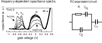
The dynamics of tunneling into self-assembled InAs dots
Self-assembled strained islands have attracted particular attention as they provide for well-defined, nanometer-size quantum dots with sizes in the 10 nm range. These systems are of great interest, not only for studying the basic properties of man-made "artificial atoms", but also because of possible device applications. Using capacitance and far-infrared spectroscopy, the many-particle ground states as well as the excitations of the dots have been investigated in the past. For possible implementation of InAs dots in future devices, it is crucial to understand the charging dynamics of these structures. We investigated the dynamics of tunneling from a three-dimensional back contact into ensembles of self-assembled InAs quantum dots by frequency-dependent capacitance spectroscopy. Apart from the influence of the tunneling barrier thickness, we investigated the influences of Coulomb blockade, magnetic fields and temperature. An equivalent resistance-capacitance (RC) circuit can be derived from the balance of charge in the device which allows us to determine the tunneling times for each state of the dots. The different tunneling times for different many-particle states are explained by a reduced tunneling barrier and Coulomb interaction. A magnetic field applied perpendicular to the tunneling direction results in a strong suppression of the charging signal, which is attributed to enhanced localization caused by the magnetic field. Calculations for 3D-0D magneto-tunneling can account for the experimental data. Our investigations show that by suitable sample design the tunneling time can be adjusted in a wide range which promises technical applications ranging from charge storage to ultrafast switching.
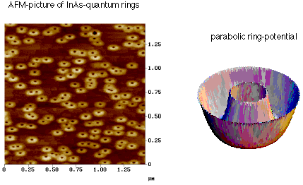
Self assembled InAs rings
Modification of the growth conditions during the fabrication of InAs-Islands can be used to create InAs-InAs-nanorings instead of dots (see fig. below). In order to demonstrate that the morphology of InAs-quantum rings like in fig. 1a translates into a ring-like electronic structure we have investigated the many-body ground states and their excitations by both capacitance and far infrared spectroscopy. These experiments show that the electronic properties are different than for dots. In particular we have observed a magnetic field induced transition of the one electron ground state and additional resonances in the excitations (compared to the two mode spectrum of quantum dots). Our results can be qualitatively explained by theoretical calculations assuming a parabolic potential as in the fig below.
A.7. SET-transistors in Silicon-on-Insolator (SOI) substrates
Etching quantum dot and quantum wire structures defined by the technique of low-energy electron-beam lithography on thin, highly doped silicon on Insulator films (about 30 nm thick) we realize quantum dot devices for the application at high temperatures.
Passivation by thermal oxidizing of the silicon structures, deposition of a thin gate oxide on top of the structure and evaporation of a metallic top-gate completes the preparation process of this SET-devices.
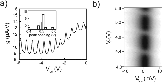
Figure 4. a) Coulomb blockade oscillations at 4 K in a highly doped silicon nanowire. b) Coulomb diamond in the same structure
In the above figure, the Coulomb blockade oscillations and the Coulomb blockade diamond observed in a highly doped SOI-nanowire at 4.2 K are shown.
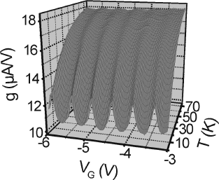
Figure 5. Temperature dependence of the Coulomb-blockade oscillations in a quasi-metallic silicon nanowire
The figure shows the temperature dependence of the top-gate controlled Coulomb blockade oscillations in an SET-transistor realized in a highly doped SOI-Quantum wire.
A. 8. Micromachined silicon devices and nanostructures
Underetching of silicon nanostructures on SOI-devices suspends the device by removing the buried oxide under the silicon film. Using this technique, we succeed in fabricating suspended, highly doped silicon nanowires and quantum dots with lateral dimensions down to 50 nm. These devices show clear deviations from ohmic behaviour. We expect to observe Coulomb-blockade on these devices in the near future, allowing also the study of electron-phonon interaction in this regime. Especially the application as a high power device seems to be obvious, since the electron-phonon interaction, leading to unwanted heat consumption, is strongly suppressed due to selection rules for scattering of electrons and acoustic phonons.
Figure 6. Suspended silicon nanowire. The cross section of this device is 80 * 140 nm.
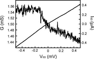
Figure 7. Conductivity of a similar suspended nanowire
Furthermore, applying the technique of epitaxial-liftoff, that is well established at our institute for GaAs/AlGaAs-structures, to the SOI-system, we built a first thin-film transistor on a 190 nm thick single-crystalline silicon film, that was removed from the SOI-substrate by underetching and stuck to a quartz substrate. The figure below shows the I-V characterisitic of this novel MOSFET structure. This technology promises applications in thin-film high-quality MOS-devices on arbitrary, especially fexible or curved substrates.
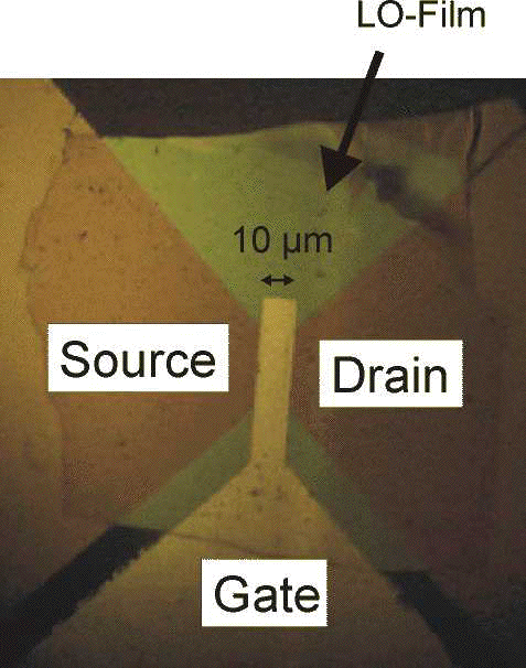
Figure 8. MOSFET in a thin single crystalline silicon film attached to quartz.
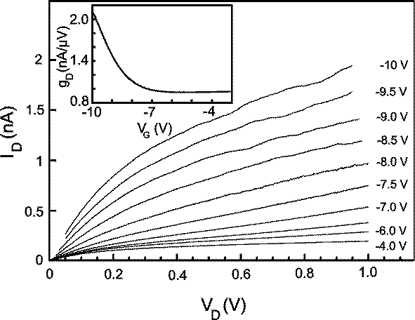
Figure 9. I-V characteristics of the bonded MOSFET
A.9. Nanomechanics
The basic idea of most sensors, such as acceleration or gas sensors, is to detect the change in the mechanical motion of a small structure electrically. Scaling down these devices to dimensions of only a few 100 nm is important for increasing speed as well as sensitivity. Moreover, studying the mechanical properties of such devices reveals interesting physics as well.
In the figure below you can see a small beam, machined out of silicon and gold. The fabrication technique is as follows: The basic material is a conventional Silicon-on-Insulator (SOI) substrate. First the structure is written with a Scanning Electron Microscope (SEM). In order to suspend the beam two etching steps are required, first dry etching, performed with an Reactive Ion Etcher (RIE), and second, wet etching, performed in diluted HF.
The sample is cooled down to 4.2 K and a magnetic field of up to 12 Tesla is applied, which is in the plane of the sample, but perpendicular to the beam. A high frequency current is driven through the beam, resulting in an inductive force out of the plane of the sample. The motion of the beam induces an electromotive force, which results in an increased absorption of electrical power. In our experimental setup, we are measuring the reflection of the signal applied. By changing the excitation frequency, we are able to detect the mechanical eigenfrequency of the beam. Low power excitation leads to a symmetric resonance curve, i.e. the resonator is in the linear regime. If the power of the excitation is increased at B = 12 T, the resonator can be driven into nonlinear response. The shape of the absorption peak is then strongly distorted and a region with infinite derivative appears.
The region of infinite derivative can be used for charge detection. The gate nearby can be charged by a negative voltage. This voltage shifts the position of the eigenfrequency of the beam and thus the position of this region. This shift can be used to determine the charge on the gate, if the charge fluctuation on the gate is minimized. In the present structure an accuracy of approximately 70 electrons was determined.
One familiar example of a device, which is working according to the principle of combining electrical and mechanical properties, is the classical bell. When scaling down such a bell, it should be possible to count electrons, which flow during each cycle of motion. In the figure below a typical structure used in the experiments is shown. A suspended, completely metallized clapper C, source-drain contacts S and D and two gates G1 and G2 are seen, which are used to drive the clapper electrostatically. Again, by changing the frequency of the excitation, the eigenfrequencies of the clapper can be determined. Due to the more complex geometry, the mechanical resonance spectrum shows response at much more frequencies. Via the simple relation I = nef (f: frequency, I: current, e: electron charge), the number n of electrons transferred in each cycle can be determined. By reducing the power of the excitation, we are able to transfer at least 7 ± 2 electrons per cycle. The reduction to one electron per cycle could be possible, if Coulomb blockade effects at low temperatures are included.
B. Intra- and Interband Spectroscopy
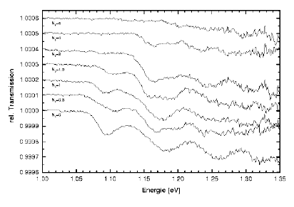
Figure 10. Interband absorption spectra of an array of self-assembled quantum dots. With increasing carrier density in the dots the energetically low-lying transitions become 'Pauli-blocked' as the final states for the transitions are already occupied by electrons. Note the extreme sensitivity of the experiment as indicated by the very small absorption measured!
B.1. Electron Systems in Band Gap Engineered Quantum Systems
Modern crystal growth techniques like molecular beam epitaxy offer the unique advantage of tailoring the band edges of different semiconductor systems in a very controlled manner. A prominent example is the so-called parabolic quantum well (PQW), but also more complex systems can be realized.
In close co-operation with the research group of A.C. Gossard in Santa Barbara we concentrate on the investigation of the collective reponse of low-dimensional electron systems in such man-made semiconductor structures.
In 1998, we focused on the investigations of the possibility to emitt far infrared radiation from such structures. As has been demonstrated by the group of Prof. Gossard, the emission from a parabolic quantum well can be triggered by a strong heating of the electron system by application of a large drift current to the carriers. The frequency of the emitted radiation nicely corresponds to the one of optical absorption, hence also obeying Kohn's Theorem. We followed an alternative route, namely to impose the strong lateral electric fields of a piezoactive surface acoustic wave onto the electron system in a PQW. Here, we also employed the hybridization technique mentioned above, where the SAW is excited on a LiNbO3 substrate and the semiconductor quantum well is deposited on top in form of a thin film.
B.2. Spectroscopy of Self-Organized InAs Quantum Dots
With decreasing sizes of nanostructures the problem of homogeneity becomes more and more important. Ideally, one would like to study large arrays of identical quantum systems. One elegant way to achieve this is to use fabrication mechnisms where the shape and the dimensions of the nanostructures are given by, energetic considerations, such that energy minimization will lead to the desired sample homogeneity. This happens, e.g. in the Stranski-Krastanow growth mode of InAs on GaAs heteroepitaxy and results in layers of uniform quantum dots of ~ 20 nm diameter and ~ 7 nm height. In a close collaboration with P. Petroff 's group at UC Santa Barbara we have demonstrated that these dots can be integrated into a metal-insulator-semiconductor heterostructure, which allows us to tune the electron number per dot, determine it by capacitance spectroscopy, and study the dots' excitation in the far-infrared. Here, the far-infrared spectroscopy resembles the atomic spectroscopy mentioned in the introduction. Indeed, we can "tune the dots through the table of elements" and distinguish, e.g. "quantum dot Helium" and "quantum dot Lithium" by their excitation spectrum. Furthermore, we can directly compare the different ground states of these few-electron systems, and, from a comparison between ground state and excitation energies, derive detailed information on the Coulomb and quantization contributions to the energetic structure of these man-made "atoms". A natural step further is the fabrication of "quantum dot molecules". This can be achieved because the Stranski-Krastanow islands tend to align when they are grown on top of each other. So far, no direct evidence for quantum mechanical coupling was observed, since the distance of the dots (10-20 nm) does not allow for a considerable overlap of the wave functions. However, the Coulomb interaction between the carriers in the different dot layers reveals itself in a distict shift of the many particle ground state energy. For the closely (10 nm) spaced dots, the charging sequence can be affected by an applied magnetic field.
B.3. Optics on Field-Effect Induced Tuneable Potential Superlattices in AlGaAs-GaAs Heterostructures.
In 1998, we continued our research on voltage - controlled lateral superlattices to demonstrate the trapping of photogenerated excitons. We were able to show that such a system may act as an efficient trap for neutral excitons and investigated the generation-, diffusion and relaxation processes in great detail.
Triggered by the success of the 'photon conveyor belt' described above, we also use static interdigitated gates to efficiently trap photogenerated charges in this potential landscape. Here, we can store optical information in an accumulative way in our laterally defined staorage cells. After some accumulation time, the optical storage cell can be switched to the 'storage mode' and finally be triggered externally to release the stored information in a flash of light. Even for a not optimized system, storage times in excess of 50 musec have been already demonstrated!
Presently, we are exploring possibilities to exploit these remarkable effects in terms of new, alternative and superior optical devices for detection, storage, switching, routing of optical signals as well as for optical signal processing like pattern recognition etc.
B.4. Intraband and Interband optics on self-assembled quantum dots
We have set up a system to measure the transmission coefficient of a sample at wavelengths around 1 micron with extremely low noise for interband experiments. The idea is to measure interband absorption through changes in the intensity of transmitted light. We have applied the technique to samples containing self-assembled quantum dots where the change in absorption is only about 1 part in 104 at resonance. Nevertheless, by using charge-tunable dots provided by P. Petroff 's group at UC Santa Barbara we have detected the transitions with good signal:noise. The charge-tunable dots have the advantage that we can load the dots with a discrete number of electrons and therefore measure the optical properties of charged excitons. The results show how the various interband transitions disappear according to the occupation of the dots (Pauli-blocking). Furthermore, there are energy shifts in the higher transitions as we occupy the electron ground-state. We are presently extending the work also to samples with two dot layers, and to dots provided by Harri Lipsanen, Helsinki which are defined with stressors. The experimental techniques to study the SAD optics are near field microscopy, Fourier-transfrom spectroscopy, and surface acoustic wave transmission experiments.
C: Nanometer Fabrication and Characterization
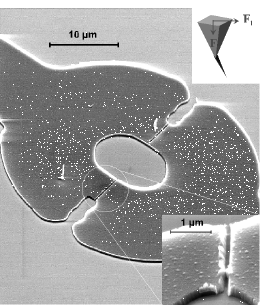
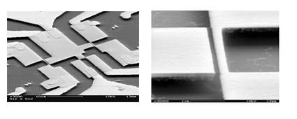
Figure 11. SEM micrograph of a double junction SQUID: The junctions are generated in the evaporated Al at the optically predefined constrictions. The lower right inset shows a magnification of one of the junctions -- it is clearly seen that all the material is removed. The upper inset shows a schematic representation of the nano-plough: the EBD tip isdeposited with an angle on a common AFM-tip, causing a vertical force when dragged through material.[20-98]
C.1. New 'Supertips' for AFM
The quality of scanning probe microscope, in particular the atomic force microscope (AFM) crucially depends on the quality of the tips used. The key features defining the quality are the radius and the aspect ratio, i.e. the geometry of the tip, as well as their durability.
Over the last years we kept on developing the so called electron-beam-deposition (EBD) further and further. Our EBD-tips combine high resolution imaging, which is at least comparable to that known from the very best silicon AFM sensors, with the extreme durability of diamond coated sensors. Furthermore they can be costum made to almost every geometry requested, ranging from 100 nm short to well over 5 µm long needles, with tip radii from a very few nanometers to some 100 nm. Even more complex sensors, e.g. hook like tips, curved needles, closed loops to name but a few, can be made upon request. Whatever the need for a tool on the nanometer lengthscale might be, EBD material can well be the material one is looking for.
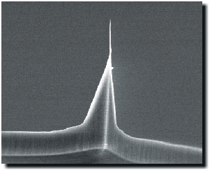
Figure 12. SEM image of a 3 µm long EBD tip, deposited onto a standard silicon AFM cantilever.
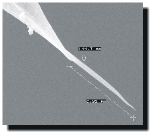
Figure 13. Close up view of the tip from the left. The tip is deposited under such an angle, that it comes normal to the sample surface. Dimensions:
- tip radius: better 5 nm
- max. thickness: less 150 nm
- length: 3 µm
These tips are perfectly suited for non-destructive characterisation and precise quantitative measurement of semiconductor nanostructures, in particular "flying", free standing structures such as (Robert, Laura, Armin, Arthur et al.) or deep trenches and holes.
The feasability of the tips in biology, medicine, biophysics, material science have been proven by a number of collaborations including the Deutsche Krebsforschungszentrum Heidelberg, Materialforschung Jena, Olympus Inc., Carl Zeiss, VEECO, Max-Planck Institut für Kolloid- und Grenzflächenforschung Berlin.
As a spin-off these activities the company NanoTOOLS GmbH was founded, which makes these tips commercially avaible.
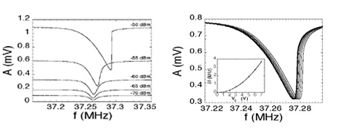
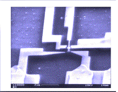
C.2. Nano-ploughed Josephson-Junctions as on-chip Radiation Sources
A new technique was developed which enables the fabrication of highly transparent Josephson junctions in combination with mesoscopic devices. We utilize a modified AFM tip to plough grooves into superconducting material, thus defining a weak link [20-98]. In reversion to the voltage-standard, the ac-Josephson effect "converts" an externaly applied voltage V to electromagnetic radiation of frequency f according to the basic Josephson equation:
f = 2e V / h
Direct mechanical structuring seems not to be the obvious method to build mesoscopic devices. Nevertheless, the main advantages of this approach are the ease of integration of the different techniques and the flexibility to build spectroscopic tools in the quantum limit. While conventional spectroscopy relies on bulky external frequency sources, here the radiation source can be placed within nanometer distance to the device under test. This not only allows the generation of high intensity electromagnetic fields exactly at the nano-structure, minimizing effects by external heating, but also spectroscopy on quantum structures and the investigation of coherent electron tunneling phenomena directly in the frequency domain.
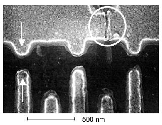
Figure 14. SEM-micrograph of a double quantum dot with an embedded nano-ploughed weak-link. The circle indicates the position of the variable thickness weak link, acting as a Josephson Junction.
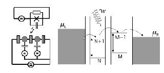
Figure 13. Schematic representation of the double dot from the left. Electron transport through the system is made possible by absorption of photons.
In the SEM image above, the weak link is made within the superconducting split-gates, which are used to electrostatically form a (conventional) double quantum dot and serves as a source of millimeter wave radiation around 100~GHz. We find that the millimeter wave emission of the weak link leads to a bolometric effect in the case of quantum point contact spectroscopy.
C.3. Direct Fabrication of Nanostructures by AFM induced Oxidation
Anodic electrochemical oxidation of metal and semiconductor surfaces is a well-established technique to grow oxides on them. For some materials, e.g. GaAs, it is the only way to oxidise them. Hereby, the metal/semiconductor is placed into an electrochemical cell, where it is biased as anode. Whereever it is exposed to the electrolyte, an oxide will be formed.
The electrochemical reaction can now be laterally confined to the dimensions of an AFM probe. Under ambient conditions, a water meniscus will be formed, which then acts as a nanometer scaled down version of the standard electorchemical set up. Again, the formation of the oxide is constricted to the exposed areas - which is now almost identical to the meniscus. Optimizing the relevant parameters such as bias voltage, exposure time, humidity to name but a few, reducing the size of the meniscus by using hydrophobic probes and compensating the electrostatic forces by working in non-contact AFM mode, the local oxidation becomes a lithographic technique allowing to define 2D, 1D and 0D insulating regions [13-98].
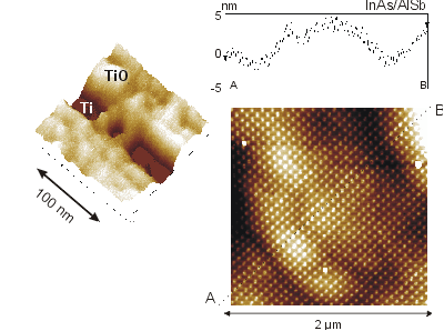
Figure 14. Oxide structures, defined by AFM induced local oxidation.
Left: Ti island, 18 x 24 nm2, seperated by TiO tunneling barriers from
the Ti leads.
Right: suqare oxide lattice on top of a InAs/AlSb surface quantum well. Here the
oxide forms an antidot lattice with a period of 80 nm.
C.4. X-ray investigations of laterally structured surfaces
For a collaboration with M. Tolan and W. Press at Kiel University we fabricate surface gratings on silicon (period: 500 nm to 1000 nm; height: 1 nm to 50 nm) using holographic lithography followed by a dry etching process [4-98]. Subsequently such gratings are covered with a thin deposit of different materials and studied by small-angle X-ray reflection from this well defined surface roughness. For the case of polymers, e.g. polystyrene or PMMA the propagation of surface roughness from the patterned silicon surface was measured by atomic force microscopy and synchroton x-ray reflection. The decay length of the surface modulation was much longer than that observed in simple liquids. By measuring the time dependence of the surface corrugation amplitude we are able to extract the surface diffusion coefficient.
A beautiful example for another successful co-operationbetween
our group and the one led by Prof. J. Peisl is the investigation of Surface
Acoustic Waves using X-ray techniques. By phase-locking a synchrotron to a SAW device
(!), we were able to spatially resolve the SAW induced lattice deformations on various
substrates. Using this exciting technique, we study for instance new transducer concepts
including focussing sound generators.
Figure 15. X-Ray representation of a GaAs sample with a surface acoustic wave present.
Also self-assembled dots have been studied using grazing-incidence x-ray diffraction. The small size-dispersion and the crystalline quality of the dots allowed for a detailed investigation of the SHAPE, SIZE, and LATTICE CONSTANT of these self-organized nanostructures. Loosely speaking, it has been possible (by diffraction techniques!) to "slice" the dots into thin layers and obtain the above quantities for each of these layers. The morphological information obtained by this "nanotomography", which cannot be gained from other techniques, is now available to test possible growth scenarios and shed light on the complex dot formation.
C.5. Low-energy electron-beam lithography
Using low-energy electrons for our ebeam-lithography and the negative electron resist calixarene, we realize lateral structure sizes down to 10 nm and even smaller. We show, that this resolution limit is achieved even with electron energies of only 2 keV. Proximity effects occuring in the regime around 40 keV are practically ruled out at these low acceleration voltages.
In addition, we show, that radiation damage on high-mobility 2DES realized in a semiconductor heterostructure is of no importance for electron energies up to 20 keV allowing the application for high-mobility (HEMT)-devices.
Using calixarene as an etching mask we fabricate nanowires and quantum dots in Silicon-on-Insulator (SOI) films. The following figure shows an example of such a structure.
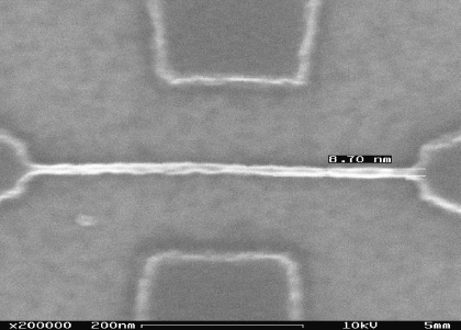
Figure 16. Silicon nanowire in a highly doped SOI-film
Guest Scientists, Visitors, and their Sponsors in 1998
- Prof. Dr. Valeri Dolgopolov (Institute of Solid State Physics, Chernogolovka,
Russia)
Volkswagen Stiftung - Dr. A.O. Govorov (Novosibirsk, Russia)
Humboldt Research Fellow and FOROPTO - Dr. Aimin Song (Beijing, China)
Humboldt Research Fellow - Prof. Dr. Sergio Ulloa (Ohio, USA)
Humboldt Research Fellow - Dr. Håkan Pettersson (Lund, Sweden)
TMR European Project
Diploma Theses completed in 1998
- Florian Hastreiter
"Gekoppelte Elektronensysteme in abstimmbaren Quantentopfstrukturen" - Tanja Elisabeth Stimpel
"Magnetotransport an kraftmikroskopisch hergestellten Modulationsübergittern in InAs-Oberflächenquantentöpfen" - Stefan de Haan
"Magnetotransport in Antidot-Übergittern mit komplexer Einheitszelle" - Christoph Bödefeld
"Interbandoptik an selbstorganisierten Quantendots" - Dirk Haft
"Nahfeldoptische Spektroskopie an Halbleiterheterostrukturen bei tiefen Temperaturen" - Ingo Tiemann
"Kontaktlose Scherkraftmikroskopie auf dem Wege zur atomaren Auflösung" - Astrid Rauchfuß
"Elektrisch leitfähige Kontaminationsspitzen für kraftmikroskopische Anwendungen" - Dominik Buchetmann
"Akustoelektrische Untersuchungen an GaAs-LiNbO3 Hybrid-Systemen" - Hilger Anton
"Magneto-Transportuntersuchungen von verspannungsinduzierten lateralen Übergittern."
PhD Theses completed in 1998
- Wolfgang Gödel
"Einzelelektronentunneln in quasi-linearen Elektroneninseln und zeitveränderlichen Feldern" - Stefan Zimmermann
"Optische Eigenschaften elektrisch abstimmbarer lateraler Potentialübergitter in Halbleiterheterostrukturen" - Barbara Miller
"Hochauflösende Kapazitätsspektroskopie an selbstorganisierten Quantenpunkten"
Publications in 1998
A. Transport Properties
- 3-98 - A. M. Song, A. Lorke,
A. Kriele, J. P. Kotthaus, W. Wegscheider, and M. Bichler
"Nonlinear Electron Transport in an Asymmetric Microjunction - A Ballistic Rectifier - "
Phys. Rev. Lett. 80, 3831-3834 (1998). - 5-98 - O. Steffens, T. Schlösser,
P. Rotter, K. Ensslin, J. P. Kotthaus, U. Rössler,
and M. Holland
"From the Two-Dimensional Electron Gas to Antidot Superlattices: Magnetoresistance Effects in the Transition Regime"
J. Phys.: Condens. Matter 10, 3859-3872 (1998) - 11-98 - B. T. Miller, W.
Hansen, S. Manus, R. J. Luyken, A. Lorke, J. P. Kotthaus,
G. Medeiros-Ribeiro, and P. M. Petroff
"Fine Structure in the Spectrum of the Few-Electron Ground States of Self-Assembled Quantum Dots"
Physica B 249-251, 257-261 (1998). - 12-98 - A. Lorke, S. Wimmer,
B. Jager, J. P. Kotthaus, W. Wegscheider, and M. Bichler
"Far-Infrared and Transport Properties of Antidot Arrays with Broken Symmetry"
Physica B 249-251, 312-316 (1998). - 15-98 - C. Dahl, P. Goy,
and J. P. Kotthaus
"Magneto-Optical Millimeter-Wave Spectroscopy"
in "Millimeter Wave Spectroscopy of Solids", Ed. G. Gruner (Springer, Berlin-Heidelberg 1998) pp. 221-282. - 16-98 - R. J. Luyken, A.
Lorke, M. Haslinger, B. T. Miller, M. Fricke, J. P. Kotthaus,
G. Medeiros-Ribeiro, and J. M. Petroff
"Electronic Coupling Effects in Self-Assembled InAs Quantum Dots"
Physica E 2, 704-708 (1998) - 21-98 - M. Rotter, W. Ruile,
D. Bernklau, H. Riechert, and A. Wixforth
"Giant Acoustoelectric Effect in GaAs/LiNbO3 Hybrids"
Appl. Phys. Lett. 73, 2128-2130 (1998). - 22-98 - J. Rychen, T. Vancura,
T. Heinzel, R. Schuster, K. Ensslin
"Commensurability Oscillations of Rectangular Antidot Arrays: A Classical Diffusion Model"
Phys. Rev. B 58, 3568-3571 (1998). - 26-98 - A. Erbe, R. H. Blick,
A. Tilke, A. Kriele, and J. P. Kotthaus
"A Mechanically Flexible Tunneling Contact Operating at Radio Frequencies"
Appl. Phys. Lett.73, 3751-3753 (1998). - 31-98 - R. J. Warburton,
B. T. Miller, C. S. Dürr, C. Bödefeld, K. Karrai, J. P. Kotthaus,
G. Medeiros-Ribeiro, and P. M. Petroff
"Coulomb Interactions in Small, Charge-Tunable Quantum Dots: a Simple Model"
Phys. Rev. B58, 16221-16231 (1998). - 32-98
- A. O. Govorov
"Structural Instabilities of the Two-Dimensional Wigner Crystal in a Lateral Superlattice"
Superlattices and Microstructures 24, 305-308 (1998). - xx-98 - V.T. Dolgopolov, A.A.
Shashkin, A.V. Aristov, D.~Schmerek, W. Hansen, J.P. Kotthaus, M. Holland,
"Nonlinear screening, spin and cyclotron gaps in the 2D electron gas of GaAs/AlGaAs heterojunctions"
Usp. Fiz.Nauk 168, 147 (1998). - xy-98 - V.T.~Dolgopolov, G.E.~Tsydynzhapov,
A.A.~Shashkin, E.V.~Deviatov, F.~Hastreiter, M.~Hartung, A.~Wixforth, K.L.~Campman,
A.C.~Gossard
"Magnetic-field-induced hybridization of electron subbands in a coupled double quantum well".
Pis'ma Zh. Eksp. Teor. Fiz. 67, 563 (1998).
B: Inter- and Intraband Spectroscopy
- 1-98
- R. J. Warburton, K. Weilhammer, J. P. Kotthaus, M. Thomas, and H. Kroemer
"The Influence of Collective Effects on the Linewidth of Intersubband Resonance"
Phys. Rev. Lett. 80, 2185-2188 (1998). - 2-98
- C. Rocke. A. O. Govorov, A. Wixforth, G. Böhm, and G, Weimann
"Exciton Ionization in a Quantum Well Studied by Surface Acoustic Waves"
Phys. Rev. B, Rapid Communications, R6850-R6853 (1998). - 6-98
- M. Hartung, A. Wixforth, J. P. Kotthaus, M. Thomas, B. Brar, and H. Kroemer
"Photoconductivity Spectroscopy of InAs/AlSb Quantum Wells"
Proc. 8th Int. Conf. "Narrow Gap Semiconductors",
Eds. S. C. Shen, D. Y. Tang, G. Z. Zheng, and G. Bauer (World Scientific, Singapore 1998) pp. 387-391. - 7-98
- W. Zawadzki, M. Kubisa, A. Wixforth, C. Gauer, J. P. Kotthaus, B. Brar,
and H. Krömer
"Spin and Depolarization Effects in InAs/AlSb Quantum Wells"
Proc. 8th Int. Conf. "Narrow Gap Semiconductors",
Eds. S. C. Shen, D. Y. Tang, G. Z. Zheng, and G. Bauer (World Scientific, Singapore 1998) pp. 289-299. - 8-98
- A. Wixforth, J. Scriba, A. Simon, C. R. Bolognesi, B. Brar, and H. Kroemer
"Density Dependence of the Spin-Splitting of the Cyclotron Resonance in InAs/AlSb"
Proc. 8th Int. Conf. "Narrow Gap Semiconductors",
Eds. S. C. Shen, D. Y. Tang, G. Z. Zheng, and G. Bauer (World Scientific, Singapore 1998) pp. 312-315. - 9-98
- S. Zimmermann, G. Schedelbeck, A. O. Govorov, A. Wixforth, J. P. Kotthaus,
M. Bichler, W. Wegscheider, and G. Abstreiter
"Spatially Resolved Exciton Trapping in a Voltage-Controlled Lateral Superlattice"
Appl. Phys. Lett. 73, 154-156 (1998). - 10-98
- Achim Wixforth
"Nano-Beben auf dem Chip: Akustische Oberflächenwellen als Photonen-Förderband"
Phys. Bl. 54, 649-653 (1998). - 17-98
- S. Zimmermann, A. O. Govorov, A. Wixforth, C. Rocke, W. Hansen,
J. P. Kotthaus, M. Bichler, and W. Wegscheider
"Voltage-Controlled Trapping of Excitons and Storage of Light in Lateral Superlattices"
Physica B 2, 35-38 (1998) - 18-98
- C. S. Dürr, R. J. Warburton, K. Karrai, J. P. Kotthaus, G. Medeiros-Ribeiro,
and P. M. Petroff
"Interband Absorption on Self-Assembled InAs Quantum Dots"
Physica E 2, 23-27 (1998) - 19-98
- A. Wixforth, C. Rocke, S. Zimmermann, J. P. Kotthaus, G. Böhm,
and G. Weimann
"Ultrasonic Light Storage in a Quantum Well: A Photon Assembly Line"
Physica E 2, 431-436 (1998). - 23-98
- C. Wiele, F. Haake, C. Rocke, and A. Wixforth
"Photon Trains and Lasing: The Periodically Pumped Quantum Dot"
Phys. Rev. A 58, 2680-2683 (1998). - 27-98
- A. Wixforth
"Nano Quakes at Work: A Quantum Conveyor Belt for Photons"
Physica E 3, 145-151 (1998). - 28-98
- F. Fuchs, E. Ahlswede, U. Weimar, W. Pletschen, H. Schmitz, M. Hartung,
B. Jager, and F. Szmulowicz
"Magneto-Optics of InAs/Ga1-xInSb Infrared Superlattice Diodes"
Appl. Phys. Lett 73, 3760-3762 (1998). - 29-98
- A. Lorke and R. J. Luyken
"Many-Particle Ground States and Excitations in Nanometer-Size Quantum Structures"
Physica B 256-258, 424-430 (1998) - 33-98
- M. Streibl, C. Rocke, A. O. Govorov, and A. Wixforth
"Novel Oproelectronic Signal Processing via the Combination of SAW and Semiconductor Heterostructures"
1998 IEEE Ultrasonics Symposium (IEEE, New York, 1998), pp. 107-110. - 34-98
- M. Rotter, W. Ruile, D. Bernklau, H. Riechert, and A. Wixforth
"Significantly Enhanced SAW Transmission in Voltage Tunable GaAs/LiNbO3 Hybrid Devices"
1998 IEEE UIltrasonics Symposium (IEEE, New York, 1998) pp.69-72.
C: Nanometer Fabrication and Characterization
- 4-98
- Z. Li, M.Tolan, T. Höhr, D. Kharas, S. Qui, J. Sokolov, M. H. Rafailovich,
H. Lorenz, J. P. Kotthaus, J. Wang, S. K. Sinha, and A. Gibaud
"Polymer Thin Films on Patterned Si Surfaces"
Macromolecules 31, 1915-1920 (1998). - 13-98 - B. Irmer, M. Kehrle, H. Lorenz, and J. P. Kotthaus
"Nanolithography by Non-Contact AFM Induced Local Oxidation: Fabrication of Tunneling Barriers Suitable for Single Electron Devices."
Semicond. Sci. Technol. 13, A79-A82 (1998). - 14-98
- R. J. Luyken, A. Lorke, A. M. Song, M. Streibl, J. P. Kotthaus, C. Kadow,
J. H. English, and A. C. Gossard
"Highly Anharmonic Potential Modulation in Lateral Superlattices Fabricated Using Epitaxial InGaAs Stressors"
Appl. Phys. Lett. 73, 1110-1112 (1998). - 20-98
- B. Irmer, R. H. Blick, F. Simmel, W. Gödel, H. Lorenz, and J. P. Kotthaus
"Josephson Junctions Defined by a Nanoplough"
Appl. Phys. Lett. 73, 2051-2053 (1998). - 24-9 - J. Cortes Rosa, M. Wendel, H. Lorenz, and J. P. Kotthaus
"Direct Patterning of Surface Quantum Wells with an Atomic Force Microscope"
Appl. Phys. Lett. 73, 2684-2686 (1998). - 25-98
- I. Kegel, T. H. Metzger, J. Peisl, P. Fratzl, A. Lorke, J. P. Kotthaus, J. M. Garcia,
P. Petroff
"Strain and Shape in Self-Assembled Quantum Dots Studied by X-Ray Grazing Incidence Diffraction"
Mat. Res. Soc. Symp. Proc. Vol. 524, pp. 89-94 (1998) - 30-98 - T. H. Metzger, I. Kegel, R. Paniago, A. Lorke, J. Peisl, J. Schulze,
I. Eisele, P. Schittenhelm, G. Abstreiter
"Shape, Size, Strain and Correlation in Quantum Dot Systems Studied by Grazing Incidence X-Ray Scattering Methods"
Thin Solid Films 336, 1-8 (1998).
Invited talks
- Khaled Karrai
"Optical absorption in Semiconductor quantum dots"
XXVII International School on the Physics of SemiconductorCompounds
(Ustron-Jaszowiec, Poland, June 7 -12-, 1998) - Jörg P. Kotthaus
"Optics of Carriers Trapped in Lateral Superlattices"
24th International Conference of the Physics of Semiconductors"
(Jerusalem, Israel, 1998) - Jörg P. Kotthaus
"Manipulating Electrons in Mesoscopic Semiconductor Devices"
MINERVA-GIF Center Symposium
(Jerusalem, Israel,1998) - Axel Lorke
"Electronic Structure of Nanometer-Size Quantum Dots and Quantum Rings"
4th International Symposium on New Phenomena in Mesoscopic Structures
(Kauai, USA, 1998) - Axel Lorke
"Mesoscopic Structures and Far-Infrared Spectroscopy"
Workshop on Far-Infrared Wave Techniques Based on Quantum Structures and Studies of Semiconductor Quantum Structures
(Tokyo, Japa, 1998) - Axel Lorke
"Many-Particle Ground States and Excitations in Nanometer-Size Quantum Structures"
13th International Confernce on High Magnetic Fields in Semiconductor Physics
(Nijmegen, The Netherlands, 1998) - Axel Lorke
"Single-Electron- and Collective Phenomena in Self-Assembled InAs Quantum Dots"
FORUM Workshop on Semiconductor Nanostructures
(Pisa, Italy, 1998) - Richard Warburton
"Confinement of Electrons and Holes in InAs Quantum dots"
Phasdom 98
(Neuchatel,Switzerland, 1998) - Richard Warburton
"Charged Excitons in InAs Quantum Dots"
17th General Conference of the Condensed Matter Division of the European Physical society
(Grenoble, France, 1998) - Richard Warburton
"Geladene Exzitonen in InAs-Quantendots"
DPG-Tagung
(Regensburg, Germany, 1998) - Achim Wixforth
"Nano-Quakes at Work: A Quantum Conveyor Belt for Photons"
10th International Winterschool on New Developments in Solid State Physics
(Mauterndorf, Austria, 1998) - Achim Wixforth
"Acoustically Driven Storage of Light in a Quantum Well"
APS March Meeting
( Los Angeles, California, 1998) - Achim Wixforth
"Nano-Beben auf dem Chip: Akustische Oberflächenwellen als Photonen-Förderband"
Pleanry talk on the march meeting of the German Physical society (in conjunction with the reception of the "Walter-Schottky-Prize")
(Regensburg, Germany, 1998) - Achim Wixforth
"Surface Aoustic Waves in Semiconductor Nanostructures"
3rd Hasliberg Workshop on Nanoscience (Swiss National Foundation and Swiss Association for NanoScience and Technology, SGNT)
(Hasliberg, Switzerland, 1998)
Financial Support
Funding of this work via the following agencies is gratefully acknowledged:
- Deutsche Forschungsgemeinschaft
- Volkswagen-Stiftung
- Bundesministerium für Bildung und Wissenschaft, Forschung und Technologie (BMBF)
- Bayerische Forschungsstiftung FOROPTO
- Alexander von Humboldt - Stiftung
- European Community Project ESPRIT and TMR
- German - Israeli - Foundation
- Siemens AG München