

Research report 2011
- Introduction
- Electronic properties
- An electron jet pump: The Venturi effect of a Fermi liquid
- Relaxation of hot electrons in a degenerate two-dimensional electron system: Transition to one-dimensional scattering
- Determination of energy scales in few-electron double quantum dots
- Quantum interference and phonon-mediated back-action in nanoscale devices
- Hyperfine Interaction in Gate-Defined Quantum Dots Incorporating a Single-Domain Nanomagnet
- Optical and optoelectronical phenomena in nanodevices
- Nanomechanical systems
- High-sensitivity interferometric detection of nanomechanical motion
- Towards detection of GHz nanoresonators
- Microwave cavity-enhanced transduction for plug and play nanomechanics at room temperature
- Nanomechanical electron shuttle
- Assembly and characterization of a high finesse fiber based optical cavity for nano-optomechanics experiments
- Cavity optomechanics and cooling nanomechanical oscillators using microresonator enhanced evanescent near-field coupling
- Probing living cells in a macro-scale transducer array based on semiconductor nanopillars
- Bachelor theses in 2011
- Master theses in 2011
- Diploma theses in 2011
- PhD theses in 2011
- Guest scientists in 2011
- Group members in 2011
- Publications in 2011
- Awards in 2011
- Invited talks in 2011
- Senior scientists of cooperating groups
- Financial support in 2011
Introduction
Chip-based nanoscale devices and systems continue to be the focus of our research aiming at both, a deeper fundamental understanding of their physical behavior in the nanometer regime and utilizing the gained knowledge for improving their functions. These include electronic devices designed to study ballistic and single electron transport, optical and optoelectronic systems controlling excitonic absorption and recombination as well as electromechanical and optomechanical systems for sensing of motion and forces but also for signal processing. We design the systems and realize them in our clean room with a broad spectrum of nanotechnological tools, in part employing heterostructures fabricated by our collaborators.
Nanoelectronic quantum transport continues to be successfully explored under the lead of Stefan Ludwig, in part embedded in the DFG-funded SFB 631 “Solid-State Based Quantum Information Processing” and the Nanosystems Initiative Munich (NIM) but also supported by individual DFG-funded grants. Optical quantum control of GaAs-based quantum dots and carbon nanotubes continues to be the major research focus of the nano-photonics group lead by Alexander Högele. Beyond his research efforts supported by the SFB 631 and NIM Alex has successfully continued collaborative projects: one with Efrat Lifshitz (Technion, Haifa) funded by the German-Israeli-Foundation on “Magneto-optical investigation of multiple excitons in blinking-free colloidal quantum dots”, one with Stefan Ludwig and Jan von Delft on “Crossover between 0.7-anomaly and Kondo effect - theory, transport measurements, and all-optical spin detection” supported by a DFG priority program, and another one with Tim Liedl and Alexander Govorov funded by the Volkswagen Foundation on “Transfer of energy and information in DNA-assembled nanocrystal networks”. The latter project recently achieved a breakthrough result published last month in Nature. Our continuing DFG-funded optical studies on ensembles of spatially indirect, dipolar excitons generated in double quantum wells and fully confined via electrostatic traps carried out again in collaboration with Alexander Holleitner at TUM complement the above nanooptical research and resulted in new and exciting insights, recently submitted for publication in three manuscripts. Our research on Nano-Electro-Mechanical Systems (NEMS), lead by Eva Weig and myself is still expanding, in part supported by the ongoing collaborative European project “Quantum Nano-Electro-Mechanical Systems” (QNEMS) coordinated by TU Delft and a DFG-funded project on “Nanoelectromechanical Resonators”. In addition Eva continues a joint project with Doris Heinrich on “Dynamic Force Field Mapping of Living Cells in a Macro-Scale Transducer Array based on Flexible Semiconductor Nanopillars” generously supported by the Volkswagen Foundation.
In our research we profit from fruitful collaborations with quite a few colleagues within the “Nanosystems Initiative Munich” (NIM) and the Center for NanoScience (CeNS) as listed below as well as former members of our group, in particular Alexander Holleitner, now at TU Munich, Khaled Karrai at attocube and also honorary professor at LMU, and Sasha Govorov at Ohio University in Athens, USA. Stimulating interactions also resulted from extended visits of former Humboldt postdoctoral fellows, such as Vadim Khrapai of the Russian Academy of Sciences in Chernogolovka, and Ivan Favero at Université Paris Diderot, and other international visitors. Our postdoctoral fellows Katarzyna Kowalik and Eric Hoffmann, supported for two years as research fellows by the Alexander von Humboldt foundation, now continue their successful research on regular postdoctoral positions at LMU. With Onur Basarir from Boston University and Darren Southworth from Cornell two additional postdocs joined us at the beginning of 2011, supported via the QNEMS project. Being embedded in both national and international collaborations further strengthens our research spectrum.
With the completion of 3 doctoral, 5 diploma, 1 master, and 8 bachelor thesis projects our educational efforts continue to be very successful. The number of 8 papers published in 2011 is quite below our recent yearly average, reflecting in part the gradually reduced size of our group as my retirement approaches quickly, but also because quite a few manuscript submitted towards the end of 2011 were published in early 2012 or still are under review. Numerous invited talks of members of our group at international conferences and workshops reflect the continued activity as well as the breadth and depth of our research efforts. Quirin Unterreithmeier, now as postdoc at Harvard, received one of the 3 prizes of the Münchener Universitätsgesellschaft for outstanding doctoral theses at LMU and Stefan Manus participated in a publication acknowledged with a CeNS publication award. Eva Weig received the prestigious Physik-Preis 2011 of the Göttingen Academy of Sciences. Not unexpected but nevertheless gratifying, all members who left our group after completing their research projects were able to obtain attractive positions with good career perspectives elsewhere.
As in previous years it is my special pleasure to thank all members of our group for their continued enthusiasm and excellent research effort. For those who have left us in 2011 I wish good luck on their new career path. With me becoming an emeritus in the fall of 2012 and my successor presently being selected from a group of highly qualified young colleagues I am looking forward to a continued bright future for the nanophysics group at LMU under new guidance. Last not least, I gratefully acknowledge the continuous generous support of our research by both national and international funding agencies. We hope that many readers worldwide enjoy this report and we are happy to receive any feedback.
Munich, April 24, 2012
Jörg P. Kotthaus
Electronic properties
Reducing the length scales of transistors well below 100 nanometers is one of the present key efforts in semiconductor industry. At the same time such tiny structures allow the observation of phenomena obeying the fundamental laws of quantum mechanics. In our clean room we fabricate a variety of gate-controlled devices by e-beam lithography starting from GaAs/AlGaAs heterostructures that contain a two-dimensional electron system (2DES). The gates lying on the sample surface can be voltage biased in order to locally deplete the 2DES. This technique allows us to further structure the 2DES and for instance create tunnel coupled zero-dimensional quantum dots or artificial molecules. In 2011 we continued and extended a number of experiments on interactions in non-equilibrium nanoscale systems, including avalanche amplification by electron-electron scattering and the transition of the latter as well as electron-phonon scattering from 2D- to 1D-systems. In a side project we established a method to accurately determine the important energy scales in double quantum dots from their stability diagrams. A spectacular experiment, which uses this method, reveals quantum interference effects in the phonon-mediated detector back-action in quantum dot circuits, where the detector is a voltage biased quantum point contact. All these experiments are related to our efforts towards quantum computing, although this connection is even clearer for our experiments on the spin dynamics of electrons confined in double quantum dots. Here we perform measurements on GaAs/AlGaAs heterostructures, a mature material system, as well as on Si/SiGe based devices which promise longer spin-coherence times, because of the possibility to get rid of nuclear spins. Our projects in 2011 relied on close collaborations with Gerhard Abstreiter (TU-München), Dominique Bougeard (University of Regensburg), Stefan Kehrein (University of Göttingen), Andy Sachrajda (NRC Canada), Geza Giedke (MPI for Quantum Optic) and Werner Wegscheider (ETH Zürich). Following we highlight a collection of our experiments:
An electron jet pump: The Venturi effect of a Fermi liquid
Daniela Taubert, Georg J. Schinner and Stefan Ludwig, in collaboration with Hans-Peter Tranitz (University of Regensburg), Werner Wegscheider (ETH Zürich), Constantin Tomaras (LMU München) and Stefan Kehrein (University of Göttingen)
A three-terminal device based upon a two-dimensional electron system is investigated in the regime of non-equilibrium transport. Excited electrons scatter with the cold Fermi sea and transfer energy and momentum to other electrons. A geometry analogous to a water jet pump is used to create a jet pump for electrons. Because of its phenomenological similarity we name the observed behavior the “electronic Venturi effect”.
The sample geometry and the fundamental concept of the electronic Venturi effect has been introduced in [1], and is described in Fig. 1. Electrons are injected at the emitter barrier (BE) with excess kinetic energy |e VE|. They scatter with electrons from the cold Fermi sea and pass on some of their energy and momentum. For a suitable collector barrier (BC) height, excited electrons can travel on toward the collector, while cold electrons are reflected at BC. The built-up positive charge between BE and BC is neutralized by electrons flowing in from the side contact.
For quantitative energy spectroscopy the collector barrier height has been calibrated in units of energy using the reflection of Landau-levels in a perpendicular magnetic field [Fig. 2(a)] [2]. A measurement of the side current - a measure of the strength of the amplification effect - is plotted in Fig. 2(b).
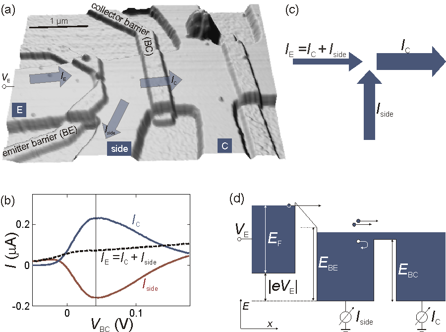
Figure 1. (a) Atomic force micrograph of the hall-bar like sample, which has been fabricated from a heterostructure containing a two-dimensional electron system by wet etching. Additional metallic gate electrodes are visible as highly elevated ares. They are used to separate emitter (E), side, and collector (C) contact. (b) Plot of the three currents indicated in (a) by arrows; the current is denoted as positive if electrons follow the arrow directions. (c) Example of actual current magnitudes (denoted by arrow width) and direction of electron flow at the position marked by a vertical line in (b). (d) Energy diagram sketching the scattering of hot electrons with the cold Fermi sea.
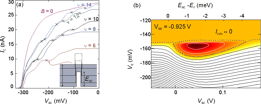
Figure 2. a) Pinch-off curves of the collector barrier BC for different magnetic fields. Due to the formation of Landau levels, plateaus in the curves emerge, which can be used to relate the barrier height in units of energy to the applied gate voltage. (b) Collector current as a function of both the gate voltage VBC applied to the collector barrier, as well as bias voltage. The area of amplification (Iside < 0) is marked by a dashed line.
- D. Taubert, G. J. Schinner, H. P. Tranitz, W. Wegscheider, C. Tomaras, S. Kehrein, and S. Ludwig, PRB 82, 161416R (2010).
- D. Taubert, G. J. Schinner, C. Tomaras, H. P. Tranitz, W. Wegscheider, and S. Ludwig, J. Appl. Phys. 109, 102412 (2011).
Relaxation of hot electrons in a degenerate two-dimensional electron system: Transition to one-dimensional scattering
Daniela Taubert, Georg J. Schinner and Stefan Ludwig, in collaboration with Hans-Peter Tranitz (University of Regensburg), Werner Wegscheider (ETH Zürich), Constantin Tomaras (LMU München) and Stefan Kehrein (University of Göttingen)
The energy relaxation channels of hot electrons far from thermal equilibrium in a degenerate two-dimensional electron system are investigated in transport experiments in a mesoscopic three-terminal device. This study is based on using the electronic Venturi effect as shown in Fig. 1 and described in Ref. [1]. A transition from two dimensions at zero magnetic field to quasi-one-dimensional scattering of the hot electrons in a strong magnetic field is observed. In the two-dimensional case, electron-electron scattering is the dominant relaxation mechanism, while the emission of optical phonons becomes more and more important as the magnetic field is increased. The observation of up to 11 optical phonons emitted per hot electron allows us to determine the onset energy of longitudinal-optical phonons in GaAs at cryogenic temperatures with a high precision to be 36.0 meV. Numerical calculations of electron-electron scattering [Fig. 2(a)] and the emission of optical phonons [Fig. 2(b)] underline our interpretation in terms of a transition to one-dimensional dynamics.
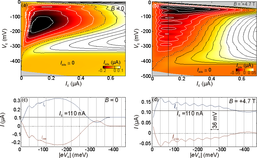
Figure 1. (a),(b) Side current versus total current and emitter bias voltage for B = 0 and B = 4.7 T. The area of amplification (Iside < 0) is enclosed by dashed lines. (c), (d) Slices at a total current of 110 nA. The oscillations in (d) are due to the emission of optical phonons, which is strongly enhanced at high magnetic field.
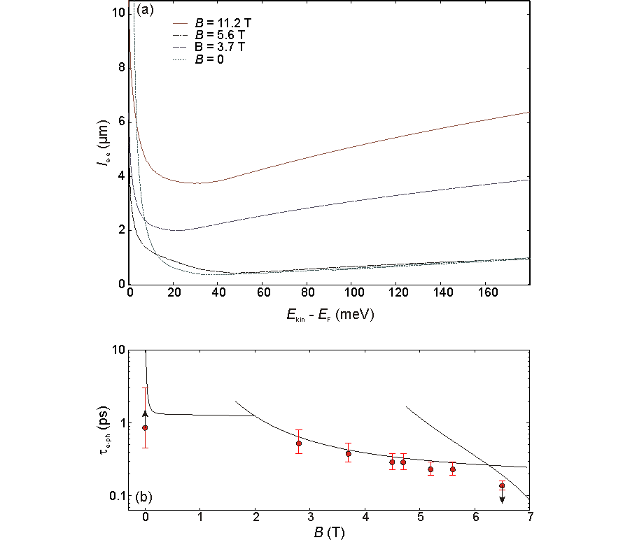
Figure 2. (a) Numerically calculated electron-electron scattering lengths as a function of excess kinetic energy for different magnetic fields. Data like those shown in Fig. 1 are consistent with these scattering length results. (b) Red disks: Electron-optical phonon scattering times estimated from experimental data. Solid lines: results of numerical calculations, describing transitions between different modes. The total scattering rate is a sum of all contributions, which is consistent with the fact that all experimental data points lie below the solid lines.
- D. Taubert, C. Tomaras, G. J. Schinner, H. P. Tranitz, W. Wegscheider, S. Kehrein, and S. Ludwig, Phys. Rev. B 83, 235404(R) (2011).
Determination of energy scales in few-electron double quantum dots
Daniela Taubert and Stefan Ludwig, in collaboration with Dieter Schuh (University Regensburg) and Werner Wegscheider (ETH Zürich)
The capacitive couplings between gate-defined quantum dots and their gates vary considerably as a function of applied gate voltages. The conversion between gate voltages and the relevant energy scales is usually performed in a regime of rather symmetric dot-lead tunnel couplings strong enough to allow direct transport measurements. Unfortunately this standard procedure fails for weak and possibly asymmetric tunnel couplings, often the case in realistic devices. We have developed methods [1] to determine the gate voltage to energy conversion accurately in the different regimes of dot-lead
tunnel couplings and demonstrate strong variations of the conversion factors.
The double quantum dot sample shown in Fig. 1(a) is measured by charge detection using the rihgt-hand side quantum point contact as detector. Optionally, an additional voltage VDQD is applied to one of the double quantum dot leads. Figure 1(b) shows the charge stability diagram for VDQD = 0, while a measurement for non-zero VDQD is plotted in Fig. 1(c). The splitting of one of the charging lines is directly related to the applied bias voltage VDQD, which therefore provides the external energy scale needed to extract the gate voltage to energy conversion.
The feature observed in Fig. 1(c) is an example for an asymmetrically tuned double quantum dot with the barrier to one lead almost closed. Figure 1(d) shows a pletora of different features related to the applied VDQD for different electron numbers and thus different coupling regimes.
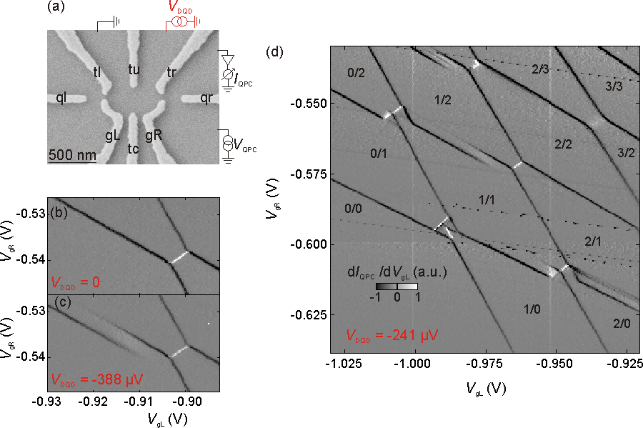
Figure 1. (a) Scanning electron micrograph of the sample structure, with charge detection circuit indicated on the right. An additional bias voltage VDQD can be applied to the right lead of the double quantum dot. (b) and (c) charge stability diagrams for VDQD = 0 and VDQD = -388 μV, showing the influence of the applied bias voltage. (d) Overview plot at non-zero VDQD for a larger area of the stability diagram, which includes several different features caused by VDQD, depending on the local coulings.
- D. Taubert, D. Schuh, W. Wegscheider, and S. Ludwig, Rev. Sci. Instr. 82, 123905 (2011).
Quantum interference and phonon-mediated back-action in nanoscale devices
Daniela Taubert, Daniel Harbusch and Stefan Ludwig, in collaboration with D. Schuh (University of Regensburg), W. Wegscheider (ETH Zürich), C. E. Young, A. A. Clerk (Mc Gill University, Montreal)G. Granger, L. Gaudreau, A. Kam, S. A. Studenikin, P. Zawadzki, Z. R. Wasilewski, A. S. Sachrajda (NRC, Ottawa)
Quantum-dot circuits are promising platforms for quantum information processing. Information readout in such systems is ultimately performed using a biased quantum point contact as a charge detector. It is crucial to understand the back-action disturbance created by this non-equilibrium detector, as it can cause decoherence. Back-action effects are complicated by the possibility of phonons mediating the exchange of energy; previous studies have shown quantum point contacts to emit phonons which are then absorbed by nearby qubits. More complexity arises in multiple dot circuits due to the possibility of interference in the interaction of electrons and phonons. We report here a pronounced back-action effect [1] where the absorption of detector-generated phonons by an undriven quantum dot circuit is strongly modified by quantum interference, and show that the effect is well-described by a theory incorporating both the quantum point contact and coherent phonon absorption. This could lead to strategies employing interference to suppress back-action effects in qubit readout.
The effect has been observed on several samples, one of which is a double quantum dot depicted in Fig. 1(a). Detector back-action appears as triangular regions in the charge stability diagrams if one of the dots is only weakly tunnel coupled to the electron reservoir [2-3]. In Fig. 1(b) an additional pattern of highly regular parallel stripes is observed. It indicates quantum interference of a phonon being absorbed either in the left or the right quantum dot as depicted in Fig. 1(c). The pattern of destructive and constructive interference arises because of the interplay between the phonon wavelength and the distance between the two dots.
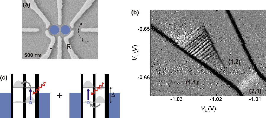
Figure 1. (a) Scanning electron micrograph of the sample structure. The quantum point contact on the right-hand side is used as a charge detector. (b) Charge stability diagram of the double quantum dot, with a large bias voltage of 1mV applied to the charge detector. A striped triangular region of detector back-action is visible. (c) Sketch of the two possible processes by which the double quantum dot can absorb an acoustic phonon. The stripes observed in (b) are caused by interference of the two processes.
- G. Granger, D. Taubert, L. Gaudreau, A. Kam, C. E. Young, S. A. Studenikin, P. Zawadzki, D. Harbusch, D. Schuh, W. Wegscheider, Z. R. Wasilewski, A. A. Clerk, S. Ludwig, and A. S. Sachrajda, in preparation.
- D. Taubert, M. Pioro-Ladrière, D. Schröer, D. Harbusch, A. S. Sachrajda, and S. Ludwig, Phys. Rev. Lett. 100, 176805 (2008).
- D. Harbusch, D. Taubert, H. P. Tranitz, W. Wegscheider, and S. Ludwig, Phys. Rev. Lett. 104, 196801 (2010).
Hyperfine Interaction in Gate-Defined Quantum Dots Incorporating a Single-Domain Nanomagnet
Gunnar Petersen, Eric A. Hoffmann and Stefan Ludwig, in collaboration with Dieter Schuh (University of Regensburg), Werner Wegscheider (ETH Zürich) and Geza Giedke (MPQ, Garching)
Double quantum dots (DQDs) laterally defined in a GaAs/AlGaAs heterostructure are well-established systems which could become the building blocks of a spin-based quantum computer. One of the remaining obstacles is the decoherence of the information carrying electron spins due to hyperfine interaction with a large number of thermally fluctuating nuclear spins. In order to investigate this interaction we have incorporated a single-domain nanomagnet on one of the electrostatic gates defining the DQD (see Fig. 1a). The nanomagnet produces an inhomogeneous magnetic field which modifies the electronic dynamics including the hyperfine interaction. We use this as a tool to study the hyperfine interaction and perform dynamic nuclear spin polarization (details of which are not discussed here) in transport measurements. Fig. 1b plots the current (color scale) through a DQD (without a nanomagnet) biased with VDQD = 0.8mV as a function of gate voltages which sweep the electronic energy levels of the dots. Due to Pauli spin blockade (see sketch) current is actually blocked even within the usually current carrying bias triangles (framed by red dotted lines). At the base of the bias triangles spin blockade is partially lifted due to the hyperfine interaction. In Fig. 1c the tiny leakage currents through DQDs with and without nanomagnet are plotted as a function of an external magnetic field Bext applied parallel to the sample surface. Without nanomagnet a single current maximum at Bext = 0 is observed. In contrast, with nanomagnet we find a broad double peak with additional sharp features. Based on similar experiments we currently study the hyperfine interaction and possibilities to manipulate nuclear spins.
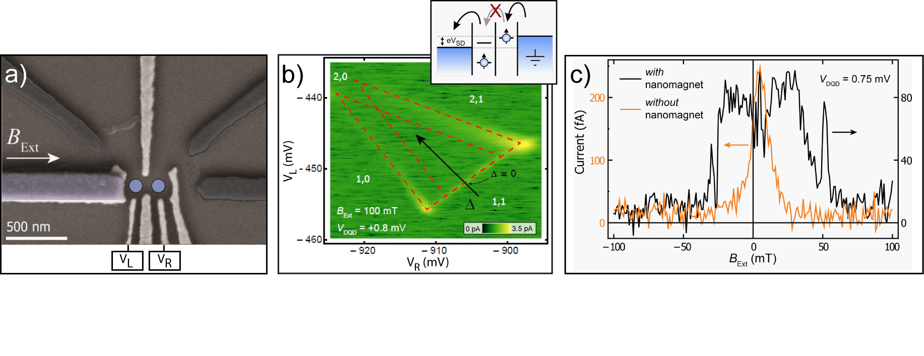
Figure 1. (a) Gate layout of the sample (scanning electron micrograph). Negative voltages on the light colored gold gates define the DQD (indicated by blue circles). The light blue gate on the left is a cobalt single-domain nanomagnet sitting directly on one of the gold gates. (b) Sequential tunneling current through the biased DQD as a function of gate voltages at Bext = 100 mT. Within the red triangles Pauli spin blockade prevents current (see inset). (c) Leakage current as a function of Bext, at finite dot energy detuning for two different samples with (black) and without (orange) nanomagnet.
Optical and optoelectronical phenomena in nanodevices
Among central topics of our research were optical studies of spatially indirect excitons in double quantum well heterostructures. In lithographically defined electrostatic traps we investigated the influence of trap configurations on the photon emission characteristics of dipolar excitons. We found enhanced emission for an excitonic antitrap compared to a trap configuration and observed an enhancement in the electrostatic tuning of the exciton energy in the antitrap-trap cross-over regime. Indirect excitons in traps were also studied at sub-Kelvin temperatures where the thermal excitonic de Broglie wavelength becomes comparable to the exciton-exciton separation. Temperature dependent studies revealed novel signatures such as strong increase in the oscillator strength with decreasing temperature and asymmetric photoluminescence spectra at very low temperatures indicating the presence of correlations among cold excitons in the trap. Studies of optical properties of carbon nanotubes and colloidal quantum dots were another research focus. Having identified limitations of commercial nanotube material we targeted in-house growth of pristine carbon nanotubes with sub-nanometer diameters and photoluminescence emission wavelengths below 1 μm that allow for optical experiments with high quantum yield detectors. We successfully established conditional growth of narrow-diameter nanotubes on silicon-oxide substrates with low enough density as required for single-nanotube spectroscopy. Initial spectroscopic characterization of the material identified a significant reduction of the spectral linewidth accompanied by an increase of the photoluminescence lifetime. We also carried out basic spectroscopy experiments on novel graded-shell colloidal quantum dots. Our investigations confirmed key features of the high quality material such as blinking-free emission and multi-exciton photoluminescence pointing towards a range of future experiments aiming at in-detail studies of the photophysics of colloidal quantum dots.
Many-body correlations of electrostatically trapped dipolar excitons
Georg J. Schinner, Enrico Schubert and Jörg P. Kotthaus
in collaboration with Andreas D. Wieck (Ruhr-Universität Bochum), Alexander O. Govorov (Ohio University) and Alexander W. Holleitner (Technische Universität München)
We perform photoluminescence measurements on electrostatically trapped dipolar excitons in an InGaAs-Double Quantum Well (DQW). As shown in Fig. 1(a) in our experimental setup the exciton generation is separated from the trapping area from which spatially resolved photoluminescence spectra are recorded. With a 3He refrigerator with a base temperature below 240 mK it is possible to cool down the trapped exciton ensemble to a regime where the thermal de Broglie wavelength becomes comparable to the exciton-exciton separation. Temperature dependent studies show a strong increase in the oscillator strengths with decreasing temperature. At low temperatures the photoluminescence spectra show an asymmetric line shape with an edge-like singularity (See Fig. 2(a)). We attribute this line shape to the strongly dipolar interaction between the bosonic excitons. Plotting the low energy side of the PL spectra logarithmically (Fig. 2(b) ) allows to extract distinct power laws I(E) ∼ (E0-E)-|α| . One of the power laws with α ≈ 0.8 disappears at higher temperatures. We interpret this disappearance of the power law in conjunction with the edge-like singularities in the PL spectra as a signature for correlated behavior of the cold exciton ensemble in the trap.
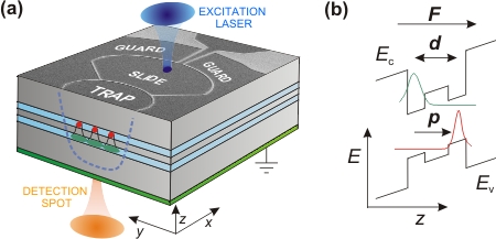
Figure 1. (a) Trapping device and detection scheme. Scanning electron microscope (SEM) image of a trap, a slide and two guard gates. (b) Schematic band diagram of the Coupled Double Quantum Well (CDQW).
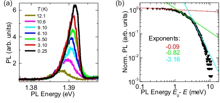
Figure 2. (a) Energy-resolved PL spectra, for different lattice temperatures. (b) Red tail of PL line shape logarithmically plotted as a function of E0 - E , with E0 being the energy of the PL maximum [TLattice = 250 mK].
- G.J. Schinner et al., arXiv: 1111.7175 (2011).
Tunable photo-emission from an excitonic antitrap
Katarzyna Kowalik-Seidl, Xaver P. Vögele, Bernhard Rimpfl, Georg J. Schinner and Jörg P. Kotthaus, in collaboration with Dieter Schuh (University of Regensburg), Werner Wegscheider (ETH Zürich) and Alexander W. Holleitner (TU München)
We study the influence of lithographically defined, electrostatic trap configurations on the photon emission from dipolar excitons in coupled quantum wells [1]. Figure 1a sketches the geometry of the devices defined on a GaAs/AlGaAs heterostructure. The photoluminescence of dipolar excitons is measured in the centre of the circular trap when VC is continuously swept from the exciton trap (VC<VG) to the antitrap (VC>VG) configuration at a fixed VG (Fig.1b). The emission is surprisingly enhanced for an excitonic antitrap compared to a trap configuration, an effect more pronounced for the smaller trap. We explain the observations by the interplay between the exciton formation process, the lateral charge-carrier dynamics, and the dipole-dipole interactions between the excitons. We detect a linear Stark-shift of the emission energy with a ratio of ΔE/ΔVC ∼30 meV/V in both trapping and antitrapping configurations, and few times enhanced ΔE/ΔVC for the voltage regime corresponding to the trap-antitrap transition (Fig.1b). We systematically analyze this effect by fitting the emission energy as a function of VC in the transition regime. Figure 1c compares the results for two devices. Thanks to the nanofabrication of the device, the energy tuning ratio is enhanced up to ∼100 meV/V, compared to the bare slope of the Stark shift of ∼30meV/V. For appropriately chosen voltage configurations the emission intensity is nearly independent of emission energy.
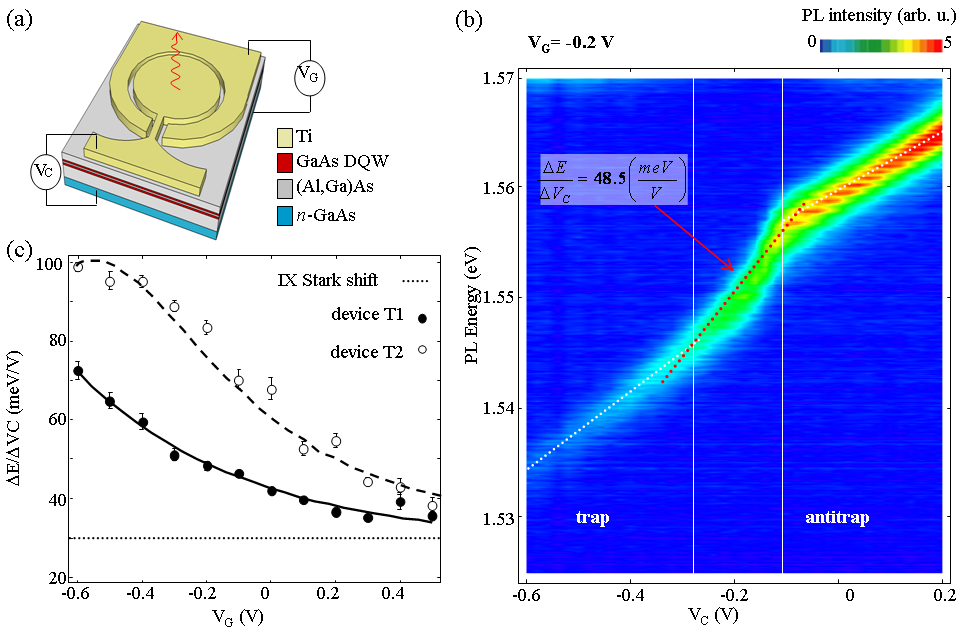
Figure 1.(a) Sketch of the trapping/antitrapping devices. Yellow: central gate C-gate with the surrounding guard gate G-gate. (b) Device T1: PL energy of indirect excitons as function of VC at VG = -0.2 V. Colour encodes the emission intensity. Vertical lines mark the transition of the trap-antitrap configuration. Dotted white lines highlight the linear Stark shift in the trap (left) and antitrap (right) configuration. The dotted red line represents a linear fit for the transition region. (c) Energy tuning ratio ΔE/ΔVC from the linear fit in the transition region measured vs. VG (device T1, C-gate diameters of 23.4 μm: closed circles; T2, C-gate diameters of 16.5 μm: open circles). Dotted horizontal line marks the slope of the Stark shift in the deep trap (VC≪VG).
- K. Kowalik-Seidl, X. P. Vögele, B. N. Rimpfl, G. J. Schinner, D. Schuh, W. Wegscheider, A. W. Holleitner, J. P. Kotthaus, Nano Lett. 12, 326 (2012).
Growth of carbon nanotubes by chemical vapor deposition
Matthias Hofmann, Jan T. Glückert and Alexander Högele
Recent photoluminescence studies of micelle-encapsulated semiconducting single-walled carbon nanotubes (CNTs) revealed that their optical properties are dominated by fluctuations in the electrostatic environment [1] and defects in the nanotube crystalline structure [2]. To minimize these effects we established growth of pristine CNTs with sub-nanometer diameters that allow for optical experiments with high quantum yield detectors. We use a home-built chemical vapor deposition (CVD) setup (Fig. 1a) with methane as the carbon feedstock and a bimetallic FeRu-catalyst that has been demonstrated to favor the synthesis of small diameter CNTs [3]. By exploring various reaction parameters we achieved controlled growth of single-walled CNTs on silicon oxide substrates with densities that are low enough to ensure single nanotube spectroscopy (Fig. 1b) and a mean nanotube diameter of 0.9 nm (Fig. 1c) required for CNT photoluminescence at wavelengths below 1000 nm.
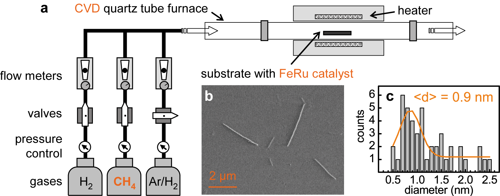
Figure 1. (a) Schematic drawing of the chemical vapor deposition (CVD) setup for the synthesis of carbon nanotubes. (b) Scanning electron micrograph of CVD-grown carbon nanotubes on silicon oxide substrate. (c) Diameter distribution of CVD-nanotubes determined by atomic force microscopy.
- K. Matsuda et al., Phys. Rev. B 77, 193405 (2008).
- T. Gokus et al., Appl. Phys. Lett. 92, 153116 (2008).
- X. Li et al., J. Am. Chem. Soc. 129, 15770 (2007).
Cryogenic spectroscopy of colloidal CdTe-CdSe core-shell quantum dots
Andre Neumann and Alexander Högele
in collaboration with G. Maikov and E. Lifschitz (Technion Institute of Technology, Haifa, Israel)Colloidal quantum dots have been studied extensively during the past decades as a paradigm of zero-dimensional systems. Celebrated for their unique optical properties such as color-tunable photoluminescence [1], conventional colloidal quantum dots are also known to suffer from nondeterministic blinking with long photo-inactive times. Recent progress in the chemical synthesis of graded-shell colloids as well as the understanding of the physical mechanisms underlying the blinking processes have culminated in the observation of blinking-free properties [2] and multi-exciton emission [3, 4]. We study core-shell CdTe-CdSe quantum dots synthesized in the group of E. Lifshitz at the Technion Institute of Technology, Haifa, Israel. Our first experiments carried out on individual colloids at cryogenic temperatures confirm the blinking-free characteristics of the high quality material and point towards more advanced studies related to the photophysics of colloidal quantum dots.
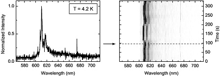
Figure 1. Photoluminescence spectrum (left) and temporal evolution (right) of a single non-blinking CdTe-CdSe core-shell quantum dot at 4.2 K.
- S. A. Empedocles and M. G. Bawendi, Science 278, 2114 (1997).
- X. Wang et al., Nature 459, 686 (2009).
- R. Osovsky et al., Phys. Rev. Lett. 102, 197401 (2009).
- H. Htoon et al., Nano Lett. 10, 2401 (2010).
Nanomechanical systems
Our research on nanomechanical systems, freely suspended nanostructures with nanoscale cross-sections and lengths of up to several 10 microns, has focussed on improving the control of their mechanical properties. In particular, a large mechanical quality factor, but also local actuation, in situ tunability of the eigenfrequency as well as highly sensitive detection over a large bandwith is desirable.
Taking advantage of our well-established doubly clamped string resonators fabricated from high stress silicon nitride, we have been able to address all above-mentioned topics: A highly sensitive Michelson interferometer has been established which allows to probe nanomechanics even at atmospheric pressure. Striving for larger eigenfrequencies, a second interferometer implementing a heterodyne mixing technique has been put into operation. Those optical detection schemes are complemented by an integrated on-chip transduction via a room temperature microwave cavity, which offers the additional benefit of tuning and manipulating the nanoresonator by means of dielectric gradient forces.
Dielectric transduction has also been incorporated into the nanomechanical charge shuttle as a well-proven tool to actuate the mechanical resonator even at cryogenic temperatures, along with a list of other improvements.
Furthermore, our effort on cavity nano-optomechanics as been enforced both in the microwave regime, where backaction-induced dynamics of a SiN resonator has been observed, and in the optical regime, where a new fiber-fased Fabry-Perot cavity quintupling the finesse has been established and new insights into near-field coupled nano-optomechanical systems have been obtained in a collaboration with Tobias Kippenberg.
Finally, nanomechanics is starting to move towards biosensing: In collaboration with Doris Heinrich, a GaAs nanopillar arry has been employed as a testbed for living cells, the fluorescence of which could be probed simultaneously with the pillar head position in a dual view microscopy setup.
High-sensitivity interferometric detection of nanomechanical motion
Johannes Rieger, Thomas Faust, Max Mühlbacher and Eva M. Weig
In nanomechanics careful sample design is vital to attain the best possible results for a specific experimental setup. Subsequent to fabrication, a fast and precise way of characterizing the mechanical resonances of the sample is thus desirable in order to quicken the whole development process.
To this end we constructed a Michelson interferometer where one mirror is closed-loop stabilized, whereas the second mirror is the actual sample itself. The high frequency intensity modulation which is caused by the deflection of the mechanical element can then be detected with a network-analyzer (Fig 1.). We achieve a displacement sensitivity of 70 fm/√Hz in vacuum and are able to detect nanomechanical motion of doubly clamped silicon-nitride beams also under ambient conditions, where the resonances are strongly damped by the surrounding gas (Fig 2.).
The high sensitivity as well as the ease of manageability make this setup a great tool for sample characterization in our nanomechanics-group.
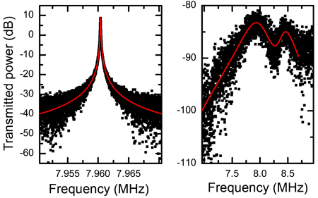
Figure 1. Amplitude of the fundamental out-of plane flexural mode of a doubly clamped silicon-nitride beam plotted versus frequency and Lorentzian fit (red solid line). Left: For a pressure of 5.8 × 10⁻³ mbar. Right: For ambient pressure. The second resonance is the in-plane mode which overlaps with the out-of plane mode because of resonance-broadening due to strong damping in air.
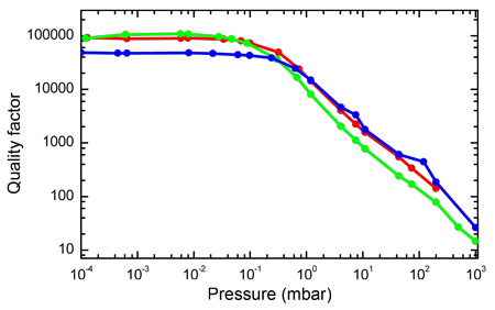
Figure 2. Pressure dependence of the mechanical quality factor of the out of plane (green) and in plane (blue) fundamental flexural mode as well as the out of plane first harmonic (red).
Towards detection of GHz nanoresonators
Onur Basarir, Jörg P. Kotthaus and Eva M. Weig
In an effort to enter the gigahertz frequency regime we have developed a Fabry-Perot type fiber optic interferometer for measuring the motion of SiN resonators. The major advantage of this detection scheme is the reduction of free space optical components and elimination of many stringent alignment steps. The interferometer has been designed to operate at telecom wavelengths near 1550 nm due to the low absorption characteristics of stoichiometric SiN around this spectral window. Thus, one can operate at higher optical power levels in order to increase the signal to noise ratio without heating the resonator considerably (Fig. 1). Also, drifts associated with temperature effects are minimized allowing for a more stable performance. Furthermore, the compact design of the interferometer allows an integration into a cryogenic measurement environment.
To increase the sensitivity of the interferometer as well as to attain higher frequencies we are currently developing a heterodyne measurement scheme. The working principle of this technique relies on mixing of the mechanical signal with a strong optical carrier and looking at the sidebands of this carrier for the mechanical signature (Fig. 2). By tuning the carrier frequency close to the mechanical resonance frequency it is possible to make the lower frequency sideband fall within the low MHz range of the r.f. spectrum where high gain amplifiers could operate easily. Thus, it might be possible to down-convert the motion of high frequency resonators and still detect them with a sufficient sensitivity.
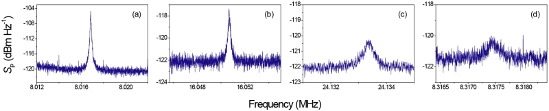
Figure 1. Power spectral density SP of a 35 μm × 300 nm × 100 nm (l × w × t) SiN doubly clamped beam measured in vacuum revealing the first three out-of-plane resonances (a,b,c) and the fundamental in-plane mechanical resonance (d). The minimum resolvable displacement sensitivity in (a) would correspond to ≅ 400 fm/√Hz at a detection power of ≅ 0.9 mW.
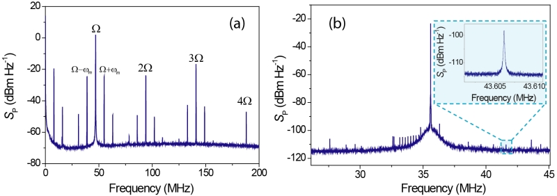
Figure 2. (a) Mixing spectrum created using an optical carrier signal modulated at Ω. The mechanical resonator is driven close to its fundamental out-of-plane resonance ωm. (b) Detection of thermomechanical motion using the mixing technique. The inset shows a zoomed-in view of the upper sideband with a Lorentzian lineshape corresponding to the mechanical resonance.
Microwave cavity-enhanced transduction for plug and play nanomechanics at room temperature
Thomas Faust, Peter Krenn, Stephan Manus, Jörg P. Kotthaus and Eva M. Weig
The readout and manipulation of nanomechanical systems can be significantly enhanced by coupling them to an optical or electrical cavity. The latter has the advantage of allowing to read out a large array of resonators with only one cavity without any positioning involved.
In this work, we present an approach based on a conventional λ/4 microstrip cavity at room temperature. It is dielectrically coupled to a doubly-clamped high stress silicon nitride beam with an extremely high mechanical quality factor of 290,000 at a mechanical resonance frequency of 6.6 MHz. Displacement detection is performed by monitoring the mechanically induced sidebands in the microwave cavity transmission signal. The sensitivity is sufficient to resolve the Brownian motion. Furthermore, the obtained coupling is strong enough to observe backaction effects of the microwave field on the mechanical resonator. We realize both cooling of the fundamental mode to 150 K as well as cavity-pumped self-oscillation. Thereby, an adjustment-free, all-integrated and self-driven resonator interfaced by just two microwave connectors is realized.
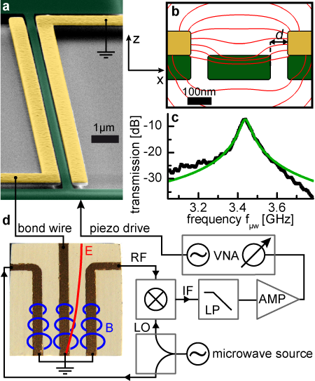
Figure 1. SEM image (a) and schematic cross section including simulated electric field lines (b) of the silicon nitride resonator and the two adjacent gold electrodes, providing the dielectric coupling. An electrical cavity with two inductively coupled feed lines (photo in d, transmission spectrum in c) is connected to the electrodes and is used to detect the mechanical motion by demodulating and amplifying the sidebands in its transmission signal.
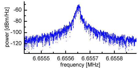
Figure 2. Using the cavity backaction, the intrinsic mechanical damping of the resonator can be overcome, leading to self-oscillation. The resulting signal, whose power spectrum is shown in the figure, has a linewidth of only 5 Hz.
- T. Faust, P. Krenn, S. Manus, J.P. Kotthaus, and E.M. Weig, arXiv.cond-mat: 1109.1156v2 (2011) and Nat. Commun. 3,728 (2012).
Nanomechanical electron shuttle
Darren R. Southworth and Eva M. Weig
The creation, measurement and control of current at the single electron level represents a natural limit of precision, and although realization of this ultimate current standard has yet to be achieved, mechanical electron shuttles provide a promising approach. Building on earlier work [1], we have designed and fabricated a mechanical shuttle the theoretical capacity to reach the single electron transport regime at reasonable temperatures.
The shuttle (Fig. 1) is composed of a gold island on a silicon nitride beam situated in a gap between source and drain electrodes. Oscillation of the beam brings the island into contact with the electrodes, and in the presence of a DC bias charging of the island results in electron transport. The island is equipped with a gate electrode and the motion of the beam can be driven dielectrically [2]. At zero bias, the small source-island and island-drain gaps (< 30 nm) as well as small electrode-island capacitance should result in charging energies that are greater than the available thermal energy at temperatures readily achievable in the lab. Careful application of a source-drain voltage then should result in electrical loading of the island, with few or single electrons transported with every oscillation of the beam, producing an exact and reproducible current.
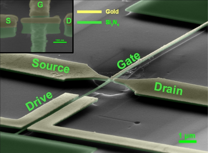
Figure 1. Scanning electron micrograph of the charge shuttle: A beam with transport island, dielectric drive electrodes as well as a local gate electrode. The inset shows the relevant island and gap dimensions, the latter being under 30 nm.
- D.R. Koenig, E.M. Weig, J.P. Kotthaus, Nat. Nanotechnol. 3, 482-485, 2008.
- Q.P. Unterreithmeier, E.M. Weig, J.P. Kotthaus, Nature 458, 1001-1004, 2009.
Assembly and characterization of a high finesse fiber based optical cavity for nano-optomechanics experiments
Sebastian Stapfner, Johannes Schmelzl and Eva M. Weig
in collaboration with Hanno Kaupp, David Hunger (LMU München and MPQ Garching), Jakob Reichel (ENS Paris), Ivan Favero (MPQ Paris Diderot 7) and Khaled Karrai (Technische Universität München and attocube systems AG)
Combining optical cavities with nanomechanical resonators allows for ultra precise detection of the resonator motion and enables to take advantage of dynamical back-action effects, where the optical field mediates the mechanical motion. Those effects increase with the quality of both mechanical and optical system, and can thus be optimized in a hybrid approach.
While high quality mechanical resonators are widely available in the nanomechanics group, a high finesse fiber-based optical micro cavity for nano-optomechanics experiments has been assembled and characterized.
The cavity is made of two optical fibers where in advance the end facets have been laser machined to obtain a concavely shaped surface and coated with a highly reflective Bragg mirror coating. Those two fiber ends were aligned with each other with respect to three translational and two rotational degrees of freedom in order to form a high finesse optical cavity. In consequence the fiber ends were glued to shear piezo elements on a monolithic platform to build a unit robust against acoustic vibrations but still tunable in a certain range by applying a voltage to the piezos. The inset in Fig. 1 shows the assembled cavity schematically where the inset in Fig. 2 depicts a photograph of the fiber ends forming the cavity.
The two orthogonal polarization modes (H and V) of the cavity are non-degenerate and separated by a few cavity line widths (Fig. 1). The cavity optical resonance line width (FWHM) was measured to be 117 MHz using sidebands with fixed frequency distance from the laser line as calibration standard (Fig. 1). The cavity free spectral range (FSR) was obtained from a white light spectrogram of the cavity to be 3.71 THz (Fig. 2). Thus the finesse was calculated to 32,000 ± 4%, such that the effective cavity length amounts to 40.4 μm including the optical mode penetrating the mirror coatings.
Compared to the previously employed cavity with finesse varying from 5,000 to 24,500 [1] the new one exhibits not only a significantly lager finesse of 32,000 but also the uncertainty in measurement of the finesse reduced to only 4%. Recently machined and coated fibers were assembled to a cavity that exhibited a finesse beyond 140,000. This progress will enhance better control and precision for optomechanics experiments.
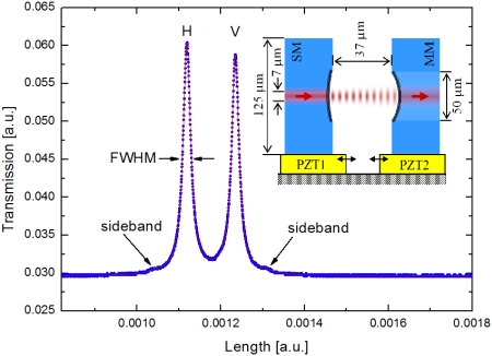
Figure 1. Cavity transmission vs. cavity length. Data points are plotted as blue dots and the red line indicates a fitted curve to the points. The cavity's two non-degenerate polarization modes (H and V) are well resolved. Sidebands modulated on the injected laser are visible as small protrusions left and right from the main resonances as indicated and serve as frequency calibration marks. Data points are plotted as blue dots and the red line indicates a sum of six Airy profiles fitted to the points. The inset shows schematically the assembly of the cavity.
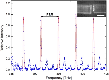
Figure 2. Transmission spectrum of the cavity when white light is injected. The cavity free spectral range is measured as the distance of the large resonances. Data points are plotted as blue dots and the red lines indicate Gaussians fitted to the points in the region of resonances. The inset shows a photograph of the two fiber ends assembled to the cavity.
- S. Stapfner et al., Proceedings of SPIE Vol. 7727, 772706 (2010) and arXiv:1110.6292v1 [physics.optics].
Cavity optomechanics and cooling nanomechanical oscillators using microresonator enhanced evanescent near-field coupling
Eva M. Weig and Jörg P. Kotthaus
in collaboration with Georg Anetsberger and Tobias J. Kippenberg (EPFL Lausanne)
In a second cavity nano-optomechanics experiment, the dispersive coupling of SiN nanostrings to the evanescent near-field of toroidal optical silica microresonators is explored. Optomechanical coupling coefficients exceeding 200 MHz/nm are found, which correspond to a vacuum optomechanical coupling rate larger than 4 kHz. A careful characterization including experimental, analytical and finite element simulation based values is performed. It is shown that both the mode-structure and -patterns of nanomechanical oscillators can be characterized relying solely on Brownian motion. Moreover, it is demonstrated that the radiation pressure interaction can cause self-sustained coherent nanomechanical oscillations at nano-Watt power levels as well as cooling of the nanomechanical oscillator. Finally, the feasibility of coupling nanomechanical motion to two optical modes where the optical mode spacing exactly equals the mechanical resonance frequency is demonstrated, allowing for Raman-type amplification and cooling of the mechanical motion.
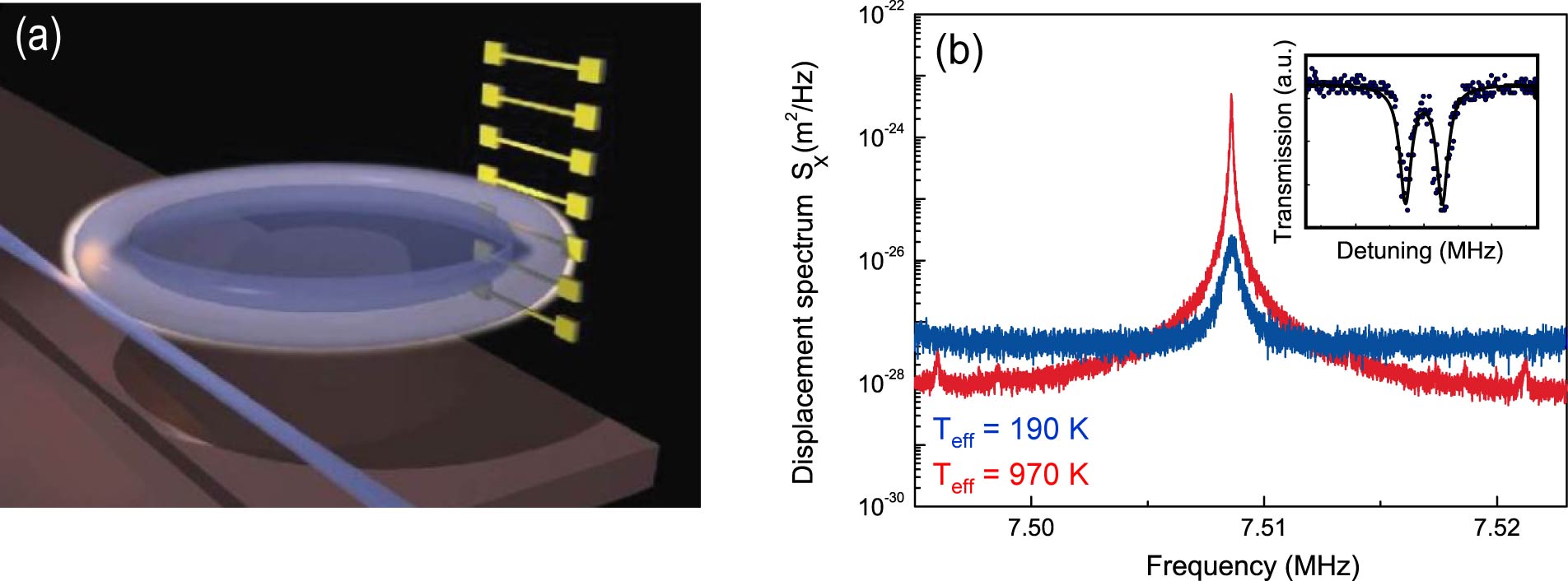
Figure 1. (a) Illustration of the hybrid cavity nano-optomechanical coupling scheme relying on the near field coupling of a nanomechanical SiN string (yellow) entering the evanescent field of the whispering gallery mode of a silica microtoroid cavity (blue). (b) Amplification and cooling using three mode coupling. The inset depicts the two employed optical cavity modes, consisting of a clockwise and counter-clockwise propagating mode doublet.
- G. Anetsberger et al., C. R. Physique 12, 800-816 (2011).
Probing living cells in a macro-scale transducer array based on semiconductor nanopillars
Philipp Paulitschke, Heribert Lorenzand Eva M. Weig,
in collaboration with Felix Keber and Doris Heinrich (LMU München)
We employ an array of flexible nanopillars vertically etched into a GaAs wafer to explore the dynamics of living cells in an artificial environment. A major goal in biosciences is the detailed understanding of cytoskeleton regulation in living cells. Actin-based force generation and cell motility is central to immune response, cancer metastasis or tissue healing and thus of basic interest for development of advanced biochemical and pharmaceutical cell assays. To reach this goal a combination of living cells (Dictyostelium discoideum) and top-down fabricated semiconductor nanopillars with well-characterized mechanical properties is employed. In order to simultaneously probe both the pillars and the cells, a dual-channel microscopy setup is established: Figure 1 shows the pillar heads in the reflection channel (blue) while cells are apparent in the fluorescence channel (green). First experiments indicate that the cells show a high cell velocity and highly directional migration behaviour most likely along channels of the periodically ordered pillar array.
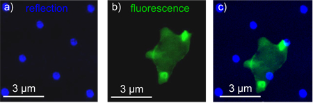
Figure 1. Colorized bright field data with the dual-channel micrograph (top view). In a) are the pillar heads (blue), in b) is the fluorescene-labelled D. discoideum cell (green) and in c) is the overlap of a) and b) shown.
Bachelor theses completed in 2011
- Christian Bourjau
“Growth and photoluminescence spectroscopy of freely suspended carbon nanotubes” - Raphael Dehmel
“Growth of Single-walled Carbon Nanotubes with Sub-Nanometer Diameters” - Lukas Hammer
“Optische Spektroskopie an in elektrostatischen Fallen gefangenen Exzitonen” - Andrej Lebedev
“Simulationen an nanomechanischen Resonatoren” - Maximilian Mühlbacher
“Interferometrische Detektion nanomechanischer Bewegung bei Raumdruck” - Stephan Pröller
“Scanning Probe Microscopy of InAs/InP nanowires” - Christian Schweizer
“Hochfrequenzfilter für Experimente im Millikelvinbereich” - Alexander Wislsperger
“Charakterisierung der optischen Eigenschaften eines faserbasierten Mikroobjektivs für Tieftemperaturmessungen”
Master theses completed in 2011
- Matthias Hauck
“Optische Spektroskopie der Wechselwirkung zwischen Quantenpunkten und ihrer elektronischen Umgebung”
Diploma theses completed in 2011
- David Borowsky
“Transportmessungen zur Untersuchung der 0.7-Struktur in Quantenpunktkontakten” - Beate Dirks
“Impact oft wo-dimensional Gold Nanoparticle Arrays on the Optoelectronic Properties of GaAs Nanowiresöpfen” - Felix Donhöfner
“Spektroskopische Untersuchung und numerische Simulation von selbst- organisierten Quantenpunkten in Feldeffekt-Strukturen ;pfen” - Peter Krenn
“Heterodyne dielektrische Detektion von nanomechanischen Resonatoren” - Wolfgang Schinner
“Spektroskopie von Kohlenstoffnanoröhren in elektrostatischen Feldern”
PhD theses completed in 2011
- Daniel Harbusch
“Hochfrequente Anregung einzelner Elektronen und Rückkopplungen eines Ladungsdetektors in gekoppelten Quantenpunkten” - Michael Olapinski
“Hochfrequenzspektroskopische Untersuchungen an Ionenkanälen in Lipidmembranen und lebenden Zellen” - Philipp Paulitschke
“Mechanische Charakterisierung einzelner und periodisch angeordneter nanoskaliger GaAs-Säulen”
Guest scientists in 2011
- Prof. Alexander O. Govorov
Ohio University, Athens, OH, USA, SFB 631 - Dr. Eric Hoffmann
Physics Department & Material Science Institute, University of Oregon, USA, Alexander von Humboldt Stiftung - Prof. Alexander Holleitner
Technische Universität München, Walter Schottky Institut - Prof. Khaled Karraï
Technische Universität München and attocube Systems AG, München - Johannes Kierig
Institut für Experimentelle und Angewandte Physik, Universität Regensburg - Andreas Wild
Technische Universität München, Walter Schottky Institut
Group members in 2011
Senior scientists
- Prof. Jörg P. Kotthaus
- Prof. Alexander Högele
- Dr. Heribert Lorenz
- Dr. Stefan Ludwig
- Dr. Eva-Maria Weig
- Dr. Onur Basarir
- Dr. Katarzyna Kowalik-Seidl
- Dr. Darren Southworth
Secretary
- Martina Jüttner
Technical staff
- Philipp Altpeter
- Anton Heindl
- Stephan Manus
- Reinhold Rath
Ph.D. students
- Thomas Faust
- Jan Tibor Glückert
- Daniel Harbusch
- Matthias Hofmann
- André Neumann
- Philipp Paulitschke
- Gunnar Petersen
- Jens Repp
- Johannes Rieger
- Georg Schinner
- Enrico Schubert
- Florian Seilmeier
- Sebastian Stapfner
- Daniela Taubert
Diploma and Master students
- David Borowsky
- Beate Dirks
- Felix Donhöfner
- Anna Eder
- Benjamin Gmeiner
- Matthias Hauck
- Peter Krenn
- Patrick Loch
- Tobias Mittereder
- Leonhard Neuhaus
- Wolfgang Schinner
- Johannes Schmelzl
- Maximilian Seitner
Bachelor students
- Christian Bourjau
- Raphael Dehmel
- Lukas Hammer
- Andrej Lebedev
- Maximilian Mühlbacher
- Stephan Pröller
- Christian Schweizer
- Alexander Wislsperger
Publications in 2011
- Leonhard Prechtel, Li Song, Stephan Manus, Dieter Schuh, Werner Wegscheider and Alexander W. Holleitner
“Time-Resolved Picosecond Photocurrents in Contacted Carbon Nanotubes” Nano Lett. 11, 269 (2011). - K. Kowalik-Seidl, X. P. Vögele, F. Seilmeier, D. Schuh, W. Wegscheider, A. W. Holleitner and J. P. Kotthaus
“Forming and confining of dipolar excitons by quantizing magnetic fields” Phys. Rev. B 83, 081307 (2011). - G.J. Schinner, E. Schubert, M.P. Stallhofer, D. Schuh, A.K. Rai, D. Reuter, A.D. Wieck, A.O. Govorov and J.P. Kotthaus
“Electrostatically trapping indirect excitons in coupled InGaAs quantum wells” Phys. Rev. B 83, 165308 (2011). - D. Taubert, C. Tomaras, G.J. Schinner, H.P. Tranitz, W. Wegscheider, S. Kehrein, and Stefan Ludwig
“Relaxation of hot electrons in a degenerate two-dimensional electron system: Transition to one-dimensional scattering” Phys. Rev. B 83, 235404 (2011). - D. Taubert, G.J. Schinner, C. Tomaras, H.P. Tranitz, W. Wegscheider, and Stefan Ludwig
“An electron jet pump: The Venturi effect of a Fermi liquid” J. Appl. Phys. 109, 102412 (2011). - D. Taubert, D. Schuh, W. Wegscheider, and S. Ludwig
“Determination of energy scales in few-electron double quantum dots” Rev. Sci. Instr. 82, 123905 (2011). - G. Anetsberger, E.M. Weig, J.P. Kotthaus, and T.J. Kippenberg
“Cavity optomechanics and cooling nanomechanical oscillators using microresonator enhanced evanescent near-field coupling” C.R. Physique 12, 800 (2011). - Omar Fakhr, Philipp Altpeter, Khaled Karrai, and Paolo Lugli
“Easy Fabrication of Electrically Insulating Nanogaps by Transfer Printing” Small 7, 2533 (2011).
Awards in 2011
- Eva Weig
Physik-Preis 2011 der Akademie der Wissenschaften zu Göttingen. - Quirin Unterreithmeier
Promotionspreis 2011 der Münchner Universitätsgesellschaft. - Stephan Manus
CeNS Publikationspreis 2011. - Stefan Ludwig
Heisenbergstipendium der DFG 2011.
Invited talks in 2011
Jörg P. Kotthaus
- “Self-oscillation in nanoelectro- and nanooptomechanical systems” Workshop on the occasion of the 60th birthday of Peter Hänggi: Noise in nonequilibrium systems: from physics to biology Dresden, Germany April 2011
- “Nonequilibrium interactions between GaAs-based quantum devices” Workshop: Nonlinear spin and charge transport through nanoscopic systems Mallorca, Spain June 2011
- “Nanomechanical resonators” Nano TR7; 7th Nanoscience and Nanotechnology Conference of Turkey Istanbul, Turkey June 2011
- “Improving Coherence and Transduction to Nanomechanical Resonators”
Workshop: Quantum to Classical Crossover in Mechanical Systems
Lorentz Center Leiden, Netherlands
October 2011
Stefan Ludwig
- “Hot Electrons on the Nanoscale: An Electron Jet Pump and the Transition from Two- to One-Dimensional Scattering” International Conference on Interactions Among Nanostructures (VCIAN) Las Vegas, USA April 2011
- “Mystery of the 0.7 Structure of Quantum Point Contacts: New Insights” NIM and CeNS Winter School 2011 St. Christoph, Austria March 2011
- “Nonequilibrium Mesoscopic Systems: Hot Electrons, Phonons & Detector Back-Action” Future Trends in Nanoelectronics Jülich, Germany June 2011
Alexander Högele
- “Quantum optics with carbon nanotubes”
Workshop on Nano Carbon Optics WNCO 2011
Herrsching, Germany
October 2011
- “Optical properties of pristine carbon nanotubes”
Hybrid Quantum Nanomaterials Workshop
TUM, Munich, Germany
November 2011
Eva M. Weig
- “Self-oscillation in nanomechanical systems” International NEMS Workshop, French Observatory for Micro & NanoTechnologies (OMNT) Toulouse, France July 2011
- “Near-field cavity optomechanics” 17th International Conference on Electron Dynamics in Semiconductors, Optoelectronics and Nanostructures (EDISON 17) Santa Barbara, USA August 2011
- “Cavitiy nano-optomechanics with hybrid devices” Workshop on Functional Hybrid Nanosystems, Institute of Advanced Study Garching, Germany November 2011
Senior scientists of cooperating groups
- Gerhard Abstreiter∗, Max Bichler
Walter Schottky Institut, TU München, Garching, Germany. - Dominique Bougeard
Institut für Experimentelle und Angewandte Physik, University of Regensburg, Germany. - Aash Clerk
Mc Gill University, Montreal, Canada. - Alik Chaplik
Institute of Semiconductor Physics, Novosibirsk, Russia. - Jan von Delft∗+
Institute for Theoretical Solid State Physics, LMU München, Germany. - Valeri Dolgopolov, Vadim Khrapay
Russian Academy of Sciences, Chernogolovka, Russia. - Ivan Favero
Université Paris Diderot, France. - Niels Fertig+
Nanion GmbH, München, Germany. - Jonathan J. Finley, Gregor Koblmüller
Walter Schottky Institut, TU München, Garching, Germany. - Hermann Gaub∗+
LMU München, Germany. - Geza Giedke
Max-Planck Institute for Quantum Optics, Garching, Germany. - Alexander O. Govorov
Ohio University, Athens, OH, USA. - Rudolf Groß+, Hans Hübl
Walter Meißner Institut, TU München, Garching, Germany. - Peter Hänggi∗
Institut für Physik, Universität Augsburg, Germany. - Theodor W. Hänsch∗, David Hunger
LMU München, Germany and Max-Planck Institute for Quantum Optics, Garching, Germany. - Achim Hartschuh∗+
LMU München, Germany. - Wolfgang Heckl∗+
Deutsches Museum, München, Germany. - Moty Heiblum
Weizmann Institute of Science, Rehovot, Israel. - Alexander Holleitner∗+
Walter Schottky Institut, TU München, Garching, Germany. - Peter Hommelhoff
Max-Planck Institute for Quantum Optics, Garching, Germany. - Atac Imamoglu
Department of Physics, ETH Swiss Federal Institute of Technology, Zürich, Switzerland. - Bernd Irmer+
Nanotools, Germany. - Khaled Karraï+
attocube Systems and LMU München, Germany. - Stefan Kehrein
Faculty of Physics, University of Göttingen, Germany. - Tobias Kippenberg∗
Max-Planck Institute for Quantum Optics, Garching, Germany and École Polytechnique Fédérale de Lausanne, Switzerland. - Don Lamb∗+
LMU München, Germany. - Tim Liedl∗+
LMU München, Germany. - Efrat Lifschitz
Technion, Haifa, Israel. - Ron Lifschitz
Tel Aviv University, Israel. - Axel Lorke+
Universität Duisburg-Essen, Germany. - Paolo Lugli∗
TU München, Germany. - Florian Marquardt∗+
Universität Erlangen, Germany. - Pierre M. Petroff
University of California, Santa Barbara, USA. - Joachim Rädler∗+, Doris Heinrich+, Bert Nickel∗+
LMU München, Germany. - Jakob Reichel
École normale supérieure, Paris, France. - Andrew Sachrajda
Institute for Microstructural Sciences, National Research Council, Ottawa, Canada. - Lukas Schmidt-Mende
Universität Konstanz, Germany. - Dieter Schuh
Institut für Angewandte und Experimentelle Physik, Universität Regensburg, Germany. - Mansour Shayegan
Princeton University, USA. - Afif Siddiki
Istanbul University, Science Faculty, Physics Department, Turkey. - Friedrich Simmel∗+
TU München, Garching, Germany. - Li Song
Shinshu University, Nagano, Japan. - Christoph Strunk
Institut für Angewandte und Experimentelle Physik, Universität Regensburg, Germany. - Philip Tinnefeld
TU Braunschweig, Germany. - Richard Warburton
Universität Basel, Switzerland. - Werner Wegscheider
Solid State Physics Laboratory, ETH Swiss Federal Institute of Technology, Zürich, Switzerland. - Andreas Wieck, Dirk Reuter
Lehrstuhl für Angewandte Festkörperphysik, Ruhr-Universität Bochum, Germany. - Achim Wixforth∗+, Hubert Krenner+
Universität Augsburg, Germany. - Wilhelm Zwerger+, Michael Hartmann, Ignacio Wilson-Rae
TU München, Garching, Germany.
+ Member of the Nanosystems Initiative Munich (NIM)
Financial support in 2011
Funding of this work via the following agencies is gratefully acknowledged: