

Research report 2004
- Introduction
- Electronic properties
- Optics with nanostructures
- Controlled motion of long-living excitons in tunable potential landscapes
- Hybridization of electronic states in quantum dots through photon emission
- Absorption spectroscopy of single self-assembled InAs quantum dots
- Exciton fine structure splitting of single InGaAs self-assembled quantum dots
- Emission from neutral and charged excitons in a single quantum dot in a magnetic field
- Voltage-Controlled Optics of a Quantum Dot
- NEMS
- Nanodevices and bio-templated nanostructures
- Diploma theses in 2004
- PhD theses in 2004
- Guest scientists in 2004
- Group members in 2004
- Publications in 2004
- Invited talks in 2004
- Senior scientists of cooperating groups
- Financial support in 2004
Introduction
Physical properties of nanoscale devices and systems continue to be the major theme of our research. In our work we combine the realization and study of top-down fabricated devices employing techniques derived from semiconductor processing with the exploration of bottom-up assembled systems made via chemical and biochemical routes. Our goals range from a deeper fundamental understanding of physical behavior in the nanometer regime to the realization of novel devices and functions developing and employing various nanotechnologies.
The study of electronic properties of nanoscale systems is motivated by the increasing importance of quantum effects as electronic devices decrease in size and by the limitations of scaling of traditional electronic devices such as the Metal-Oxide-Semiconductor Field-Effect-Transistor (MOSFET). Our studies of quantum phenomena aim at finding new ways of information processing. One current major research theme are ways to implement and control quantum bits on the basis of solid state electronic and optical devices and thus lay the ground work for a future quantum information technology. In part this research is embedded in the SFB 631 - a long term research platform on “Solid-State Based Quantum Information Processing”, funded by the German Science Foundation (DFG) since July 2003. In addition we participate in a new five-year research program on “Nanoelectronic semiconductor structures for the quantum information technology” (NanoQuit) funded by the German Ministry for Education and Research (BMBF) with research on “Quantum control in suspended semiconductor nanostructures” (QuBridge).
Though MOSFET-based Silicon technology will continue to dominate electronics for at least another decade the search for alternative approaches to electronic functions employing molecular scale units and mechanisms of self-assembly is our motivation for new research projects studying molecular electronics with carbon nanotubes and self-assembled monolayers as well artificial molecular networks and machines based on DNA-directed self-assembly. A major portion of this research is part of a DFG-funded Emmy-Noether junior group headed by Friedrich Simmel.
In the nanometer regime electronic, mechanical and optical properties become often inseparably connected. Therefore we have in recent years increased our activities on studying Nano-Electro-Mechanical Systems, in short NEMS, ranging from fundamental studies of the resonant behavior of nanoscale bridges fabricated out of semiconductors to their development as sensing and actuating devices. Ways to efficiently drive such nanoscale resonators by electric, magnetic, mechanic as well as optically induced forces are one current research aspect. Sensing the mechanical motion with nanometer resolution via capacitance, current or optical reflection is another basic theme of ongoing research.
The particular optical properties of nanoscale systems are most dramatically reflected in the discrete optical emission and absorption spectra of quantum dots. There our research is focused on studying individual quantum dots grown by a self-assembling molecular beam epitaxy process in the group of Pierre Petroff, our long-term collaborator and Humboldt award recipient at UC Santa Barbara. In these studies we employ successfully the possibility of changing the occupation of such self-assembled quantum dots with individual electrons by a gate voltage, a technique developed ten years ago in this collaboration. This is combined with high resolution optical techniques to enable the detailed study of the optical absorption and emission of individual quantum dots as a function of charge, magnetic field and temperature. The fundamental aspect of this research carried out jointly with the group of former CeNS member Richard Warburton at Heriot-Watt University in Edinburgh aims at understanding many body interactions in quantum dots. A more application-oriented goal is the realization of single photon emitters that can generate individual photons on demand and are needed for quantum information processing. Another aspect concerns the manipulation of electron-hole separation and excitonic recombination in voltage-tunable traps.
Reflecting the success of our research effort our group again changed quite a bit in 2004. Four doctoral students have completed their degree and left for attractive industrial or postdoctoral jobs. From the eight graduate students finishing their diploma in 2004 three have decided to continue with us as doctoral students, whereas one has adventurously left for doctoral research in Tokyo with our alumnus Prof. Susumu Komiyama as his advisor. Vadim Khrapay from Chernogolovka joined us in July of 2004 as recipient of a research award by the Alexander von Humboldt foundation. We wish good luck to Wendy Dittmer (neé Huynh), also a Humboldt awardee, who took up an attractive position with Philips research in Eindhoven after two years of fruitful research in our group. We congratulate Sasha Govorov, now Professor for Theoretical Physics at Ohio University, for receiving a prestigious Bessel Award by the Alexander von Humboldt foundation enabling him to continue joint research projects with us.
Members of our group presented an impressive 22 invited talks at international conferences and workshops and we have successfully published 36 papers in internationally acknowledged journals. We are also happy to report that the four start-up companies Advalytix AG, Attocube Systems, Nanion Technologies GmbH and Nanotools GmbH that were formed in recent years by members of our group increase their business success in a highly competitive world and continue to hire graduates from our group.
After celebrating a quarter of a century as the “Semiconductor Group” with a glorious skipper party on Lake Starnberg in May of 2004, attended by nearly all former and present doctoral students, we have rejuvenated as the “nanophysics group” adjusting for the continuous change of focus from semiconductor physics to the more general direction of developing systems and studying condensed matter physics in the nanometer regime. We hope that this report finds many interested readers and enjoy to use this opportunity to thank our many cooperating partners worldwide as well the generous funding bodies that make our effort in research and education possible. Any feedback our readers may have is welcome.
Munich, April 25th, 2005
Jörg P. Kotthaus
Electronic properties
The ongoing progress in quantum information processing calls for the realization of scalable and controllable solid state based systems. Lateral quantum dots defined in the two-dimensional electron gas of a GaAs/AlGaAs heterostructure are promising candidates for the implementation of such solid state quantum bits. Our investigations of single electron transport through quantum dots aim at realizing well-defined charge and spin states at low temperatures. Manipulation of the coupling between adjacent quantum dots requires few-electron quantum dots. The charge state of these artificial molecules can then be read out by means of integrated quantum point contacts. We successfully fabricated a serial double quantum dot and demonstrated full charge control in the few electron limit. For the case of the double quantum dot charged with only one electron we undoubtedly determined the interdot tunnel splitting by means of transport spectroscopy at finite bias voltage. Another aspect of our work deals with the coupling of quantum dots to the solid state environment. In order to gain control of phonon-mediated dephasing processes, a lateral quantum dot has been integrated in a free-standing nanobridge. Due to its strongly confined acoustic spectrum the nanobridge is a realization of a phonon cavity. The modified electron-phonon coupling becomes apparent in a phonon blockade of single electron tunneling. This can be understood in a model based on the Franck-Condon principle. Besides our studies on single dot phonon cavities we seek to implement double quantum dots into free-standing beams. Electronic transport measurements were also carried out in organic semiconductors, such as pentacene thin film transistors (TFTs). The samples were prepared in close collaboration with Stefan Schiefer and Bert Nickel from Lehrstuhl Rädler who also performed X-ray scattering measurements in order to shed light on the relationship between the structural and the electronic properties of pentacene TFTs. The mobilities in these TFTs could be improved by several orders of magnitude by chemical functionalization of the contacts with a self-assembled monolayer.
Quantum dots as quantum bits
Daniel Schröer, Stefan Ludwig, and Jörg P. Kotthaus, in cooperation with Karl Eberl and Werner Wegscheider
We create lateral quantum dots by depleting the two-dimensional electron system of an AlGaAs/GaAs heterostructure with lithographically defined Schottky gates. The advantage of this lateral approach is the flexibility in number and orientation of leads and gates. Multiple quantum dots can be coupled capacitively or via tunnel barriers. The interdot coupling strengths and the number of electrons per dot are tunable by means of gate voltages.
A double quantum dot is often regarded as an artificial molecule, as the discrete states of both dots split into molecular bonding and antibonding states. These form a two-level system that is applicable as a qubit for quantum information processing [1]. The complexity of the molecular states increases with the number of free electrons per dot. Hence, we aim to reduce the dot sizes and integrate suitable tools to read out the number of charge carriers (e.g. a quantum point contact; see fig. 1). The molecular states are probed by analysing the charging diagram of the system. In addition we will attempt to couple more than two quantum dots to study the interaction of several qubits.
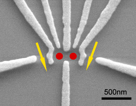
Figure 1. SEM micrograph of a sample: Surface of an AlGaAs/GaAs heterostructure (dark) with gold gates (light gray), that allow to locally deplete the 2DES and thus define two tunnel coupled quantum dots (red) and two quantum point contacts (QPC) on the sides (yellow arrows).
- Blick R. H. and Lorenz H., Proc. IEEE Symp. Circuits and Systems, II-245 (2000)
Direct control of the tunnel splitting in a one-electron double quantum dot
Andreas K. Hüttel, Stefan Ludwig, and Jörg P. Kotthaus, in cooperation with Karl Eberl.
Extending our previous work on coherent transport through coupled quantum dots summarized in [1] we have electrostatically defined a double quantum dot (DQD) at strong interdot coupling containing N=0,1,2,... electrons. Fig. 1(a) displays an electron micrograph of the gate electrodes on top of a AlGaAs / GaAs heterostructure; the position of the DQD and the current path in the two-dimensional electron gas is schematically indicated. A quantum point contact nearby serves as charge detector. It provides proof for the complete depletion of the DQD [2]. Fig. 1(b) shows single electron tunneling current through one-electron states at finite source-drain voltage USD across the DQD, plotted as function of average chemical potential of both dots Σ=(µL+µR)/2 and potential asymmetry Δ=(µL-µR)/2. Here the quantum-mechanical tunnel splitting 2t0 of the double potential well becomes visible as a pronounced anticrossing of ground and excited state in dependence on the potential asymmetry. Comparison of the anticrossing with USD allows to determine the size of the tunnel splitting. The latter has been tuned within 0.03 meV =< 2t0=< 0.3 meV by varying gate voltages or applying a magnetic field [2].
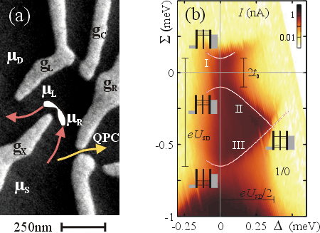
Figure 1. (a) Gate structure on top of an AlGaAs/GaAs heterostructure; the position of the double quantum dot and the current paths are indicated. (b) Single electron tunneling current through one-electron states as function of average chemical potential Σ and potential asymmetry Δ. The solid lines are model curves [2].
- H. Qin, A. W. Holleitner, A. K. Hüttel, R. H. Blick, W. Wegscheider, M. Bichler, K. Eberl, and J. P. Kotthaus, Phys. Stat. Sol. 1, 2094 - 2110 (2004).
- A. K. Hüttel, S. Ludwig, K. Eberl, and J. P. Kotthaus, cond-mat/0501012, submitted for publication (2004).
Effects of phonon quantum confinement in lateral quantum dots embedded in free-standing nanostructures
Eva M. Weig (neé Höhberger), Clemens Rössler, Stefan Ludwig, Jörg P. Kotthaus, in cooperation with Robert H. Blick, Werner Wegscheider and Dieter Schuh
The ongoing research on the transport properties of lateral quantum dots embedded in free-standing nanostructures has allowed deeper insight into the electron-phonon coupling in the limit of single electrons interacting with individual phonon modes. Our device consists of a freely suspended 130 nm thin beam of a GaAs/AlGaAs heterostructure sustaining a low-dimensional electron gas in which a lateral quantum dot was defined by gate depletion. The transport spectrum shows clear Coulomb diamonds that display an energy gap (denoted ε in Fig. 1) around the diamond centers. The underlying suppression of single electron tunneling around zero bias can be traced back to an effect named phonon blockade based on the well-known Franck-Condon principle.
In an effort to enable a more detailed investigation of phonon blockade and related effects we successfully advanced the processing of suspended nanostructures in our cleanroom . This allows the fabrication of optimized sample structures involving free-standing nanobridges incorporated within an improved gate geometry (Fig. 3). Applying negative voltages to individual gate electodes will ultimately permit control of the transport properties of the electron-phonon cavities.
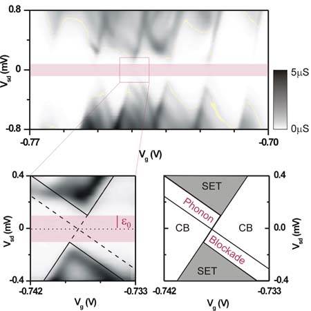
Figure 1. Differential conductance of the free-standing quantum dot as a function of gate as well as bias voltage measured at a bath temperature of 10 mK. The transport spectrum shows Coulomb diamonds with an energy gap around zero bias that is induced by phonon blockade of single electron tunneling.
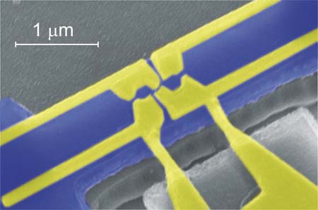
Figure 2. Gate-defined quantum dot structure embedded in a free-standing nanobridge.
- Weig E. M., Blick R. H., Brandes T., Kirschbaum J., Wegscheider W., Bichler M., and Kotthaus J. P., Phys. Rev. Lett. 92, 046804 (2004).
Optical and electronic transport properties of pentacene thin film transistors
Nok Tsao, Udo Beierlein in cooperation with Stefan Schiefer and Bert Nickel
Organic thin film transistors (TFTs) were fabricated in top and bottom contact geometry and the electronic transport as well as the photocurrent were measured. Evaporation of thin pentacene films onto silicon chips and characterization of the samples by X-ray scattering was carried out in the group of Bert Nickel. The mobility of the pentacene TFTs was successively enhanced up to m=0.5 cm2/Vs by improving the preparation parameters and by functionalization of the gold contacts with a self-assembled monolayer of short chain alkane thiols.
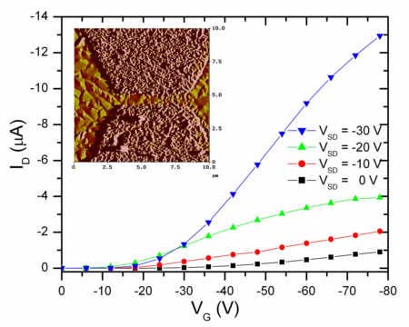
Figure 1. Drain current as a function of gate voltage of a pentacene TFT. Inset: AFM image of two gold electrodes covered with a pentacene film.
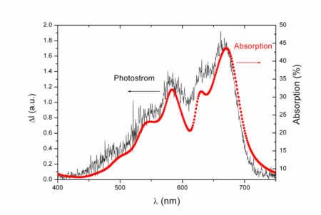
Figure 2. Photocurrent spectrum of a pentacene TFT and absorption spectrum of pentacene on glas.
Optics with nanostructures
Excitons in self-assembled quantum dots constitute another atomic-like solid state system ideally suited to study quantum properties and attractive for storing qubits. Here we combine our know-how of filling quantum dots with well-defined exciton and electron occupation with the expertise developed to perform a range of luminescence and absorption experiments on individual quantum dots. Electron-occupation dependent fine-structure of the luminescence nicely reflects the quantum nature of the charged excitonic states as well as their interaction with a nearby two-dimensional electron system. Absorption spectroscopy on individual quantum dots enabled by Stark-shift modulation spectroscopy yields quantitative insight lifetime broadening and oscillator strength of excitonic transitions and charge-tunable exchange coupling. In an international collaboration our experimental studies are complemented by theoretical efforts aiming to understand the interaction between excitons in the dot and a nearby Fermi sea. We also develop methods to trap long-living spatially indirect excitons in a double quantum well into defined lateral potential geometries ranging from 1D stripes to fully confining excitonic traps. The experiments aim at a better understanding of the temporal and spatial dynamics of such long-living excitons. In similar devices containing a single quantum well we have utilized the reversible spatial separation of optically generated electron-hole pairs via two-dimensional electrostatic potentials to create a photonic camera. This enables us to store and modify whole pictures for times up to seconds before being reemitted as excitonic luminescence.
Controlled motion of long-living excitons in tunable potential landscapes
Andreas Gärtner, and Jörg P. Kotthaus, in cooperation with Dieter Schuh
Systems of cold and long-living excitons (bound electron-hole-pairs) in coupled quantum well (QWs) structures are expected to exhibit remarkable phenomena, e.g. Bose-Einstein-Condensation [1]. This project aims to obtain a profound understanding of the dynamics of excitons by creating artificial potential landscapes for excitons. In our epitaxially grown GaAs/AlGaAs heterostructures containing a system of two QWs coupled by a thin tunnel barrier we are able to create long-living, spatially indirect excitons. They show a dramatically increased half-lifetime of 250ns under the influence of an electrical field which is deduced from spectrally and temporally analyzing the recombination photoluminescence (PL). Lithographically patterned gate structures allow us to tailor the excitonic potential landscapes via the quantum confined Stark effect (QCSE) [2]. We are able to laterally drive long-living excitons in artificially induced tunable gradient potential landscapes. The drift exceeds macroscopic distances exceeding 150µm (see Fig. 2). Using additional SiO2-patterns we created artificial ring-shaped traps for excitons as SiO2-covered regions exhibit flat-band conditions after illumination [3].
Figure 1. Sketch of the formation of a long-living indirect exciton taking place in a coupled QW structure. The strength of the applied electrical field along the z-axis controls excitonic lifetime as well as the excitonic energy via the QCSE.
Figure 2. A gradient potential is created forming a "slide" for excitons. The excitonic drift starts at the point of optical creation (black circle in the center of the figure) and continues to the left.
- see e.g. Butov et al., Nature 417, 47 (2002)
- Zimmermann et al., Phys. Rev. B 56, 13414 (1997)
- J. Krauß et al., Appl. Phys. Lett. 85, 5830 (2004)
Hybridization of electronic states in quantum dots through photon emission
K. Karrai, R. J. Warburton, C. Schulhauser, A. Högele, in cooperation with A. O. Govorov, B. Urbaszek, E. J. McGhee, J. M. Garcia, B. D. Gerardot, P. M. Petroff.
The self-assembly of semiconductor quantum dots has opened up new opportunities in photonics. Quantum dots are usually described as 'artificial atoms', because electron and hole confinement gives rise to discrete energy levels. This picture can be justified from the shell structure observed as a quantum dot is filled either with excitons (bound electron-hole pairs) or with electrons. The discrete energy levels have been most spectacularly exploited in single photon sources that use a single quantum dot as emitter. At low temperatures, the artificial atom picture is strengthened by the long coherence times of excitons in quantum dots, motivating the application of quantum dots in quantum optics and quantum information processing. In this context, excitons in quantum dots have already been manipulated coherently. We have shown [1] that quantum dots can also possess electronic states that go far beyond the artificial atom model. These states are a coherent hybridization of localized quantum dot states and extended continuum states: they have no analogue in atomic physics. The states are generated by the emission of a photon from a quantum dot. We showed [1] how a new version of the Anderson model that describes interactions between localized and extended states can account for the observed hybridization.
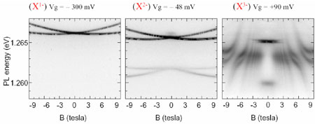
Figure 1. Photoluminescence from charged excitons. Data are shown for singly (a), doubly (b) and triply (c) charged excitons, all from the same quantum dot, versus magnetic field. The photoluminescence (PL) is represented with a grey-scale, and the magnetic field is applied perpendicular to the quantum dot plane. The InAs quantum dots are grown in the Stranski-Krastanow mode on GaAs with an annealing step at the growth temperature in order to increase the ensemble PL energy from 1.1 to 1.3 eV. Experimental details in [1,2].
- K. Karrai, R. J. Warburton, C. Schulhauser , A. Högele, B. Urbaszek, E. J. McGhee, A.O. Govorov, J. M. Garcia, B. D. Gerardot and P. M. Petroff, Nature (London) 427, 135 (2004).
- C. Schulhauser, R. J. Warburton, A. Högele, K. Karrai, A. O. Govorov, J. M. Garcia, B. D. Gerardot and P. M. Petroff, Physica E 21, 184 (2004).
Absorption spectroscopy of single self-assembled InAs quantum dots
B. Alén, R. J. Warburton, F. Bickel, and K. Karrai in cooperation with P. M. Petroff, J. Martínez-Pastor
Excitonic transitions of single InAs self-assembled quantum dots have been directly measured at 4.2 K in an optical transmission experiment. We use the Quantum Confined Stark Effect to tune the exciton energy of a given electronic state into resonance with a narrow-bandwidth laser and therefore probe its absorption [1]. With this method, the oscillator strengths as well as the homogeneous linewidths of the single dot optical transitions are obtained. Saturation spectroscopy performed on the excited and ground state revealed different energy relaxation schemes for both electronic shells. In the ground shell radiative recombination takes place leaving the electronic state ready for a new absorption. In this case, the signature of the saturation corresponds to a two level system driven by a strong external electromagnetic field [2]. On the other hand, an intermediate state is necessary to explain the saturation behavior of the absorption in the excited state. The relaxation to this state determines the exciton dephasing time (~50 ps) and can be extracted from the linewidth of the absorption resonance [1, 3]. Furthermore, a shelving model can be applied to investigate this latter case and to determine the cycling time for the full relaxation path (see figure below). We have found an average cycling time of 3 ns that can not be explained only accounting for the radiative recombination in the ground state (~1 ns). Therefore, we propose that the relaxation in the conduction band is slowed down due to Pauli blocking of the triplet state after photon emission. The restoration of the initial state needs a spin-flip in the p-shell which is responsible for the long cycling time observed in this case [3].
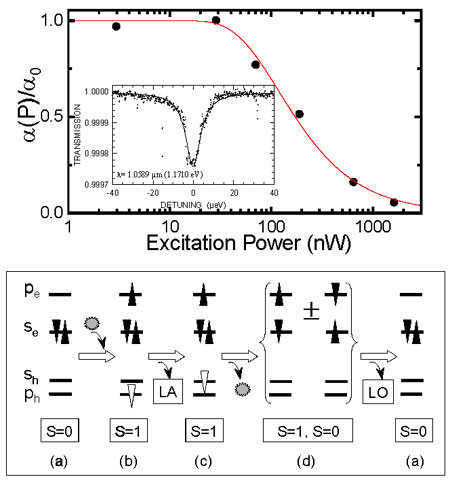
Figure 1. (Top) Evolution of the absorption amplitude of the excited state as a function of incident power. The solid line corresponds to the prediction of the shelving model with a cycling time of 3 ns. The inset shows a typical absorption spectrum in the limit of low power. (Bottom) The relaxation path for the electron and hole is depicted. An electron-hole pair is created in an initially doubly charged quantum dot. Restoration of the initial state involves sequentially the relaxation of the hole, the photon emission, and the relaxation of the electron in the singlet (fast) or triplet (slow) state.
- B. Alén et al., Appl. Phys. Lett. 83, 2235 (2003).
- A. Högele et al., Phys. Rev. Lett. 93, 217401 (2004).
- B. Alén et al., Physica E 21, 395 (2004)
Exciton fine structure splitting of single InGaAs self-assembled quantum dots
A. Högele, B. Alén, F. Bickel, S. Seidl, M. Kroner, R. J. Warburton and K. Karrai, in cooperation with P. M. Petroff.
Non-resonant photoluminescence spectroscopy on single self-assembled quantum dots has been successfully exploited in our group investigating effects of excess charge on exciton energy. Recently, the resonant absorption technique has been established for the first excited state of excitons confined in a single InAs quantum dot [1]. Absorption spectroscopy is a powerful technique as it measures directly the linewidth of a transition as well as the electric dipole moment. Absorption spectra were obtained by sweeping the exciton energy into resonance with laser photons through voltage induced Stark-shift. The absorption spectroscopy technique was extended to the ground state of a neutral exciton confined in a single self-assembled InGaAs quantum dot [2]. The resonant transition was directly observed in an optical transmission experiment. A spectrum of the differential transmitted intensity is shown in Fig.1 (b) and compared with the corresponding photoluminescence spectrum (a). With the novel spectroscopic approach the experimental spectral resolution was improved by more than two orders of magnitude down to ~ 1 µeV revealing the fine structure splitting of the neutral exciton (c). In addition to the fine structure splitting an upper bound on the homogeneous linewidth at 4.2 K and the transition electric dipole moment were determined.
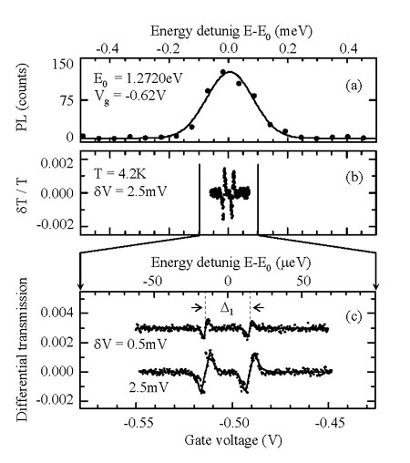
Figure 1. (a) Photoluminescence spectrum of the neutral exciton in a single quantum dot. The spectral resolution is limited by the spectrometer to 150µeV. (b) Differential transmission spectrum of the neutral exciton on the same quantum dot showing two resonances. (c) Zoom-in representation of (b) by factor of 10 in energy. The fine structure splitting between the resonances is 30µeV.
- B. Alén et al., Appl. Phys. Lett. 83, 2235 (2003).
- A. Högele et al., Physica E 21, 175 (2004).
Emission from neutral and charged excitons in a single quantum dot in a magnetic field
C. Schulhauser, R. J. Warburton, A. Högele and K. Karrai, in cooperation with A. O. Govorov, J. M. Garcia, B. D. Gerardot and P. M. Petroff.
A novel technique for performing single dot spectroscopy at low temperature and at high magnetic fields was presented. We reported on the performance of our fiber based microscope which has the advantage that the spot position does not change in magnetic field with respect to the sample. Example results on the magneto-PL from charged excitons in an individual dot were also presented. The neutral, singly-charged and doubly-charged excitons exhibit a spin Zeeman effect and diamagnetic shift in magnetic field which are characteristic of a strongly localized emitter. We found however that the triply-charged exciton behaves quite differently, exhibiting a series of anti-crossings periodic in 1/B [1, 2]. We demonstrated that this cannot be related to Shubnikov-de Haas oscillations of electrons in the wetting layer [2]. The results confirm that a hybridisation of quantum dot and unoccupied Landau levels takes place.
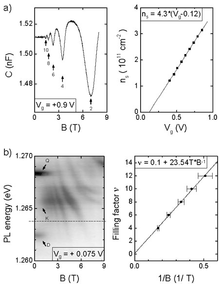
Figure 1. (a) Magneto-capacitance measurement on an ensemble of QDs. Left: Occupation of Landau levels is indicated with arrows and labelled by the filling factor. Right: Two-dimensional electron gas density versus gate voltage as determined from the magneto-capacitance. (b) Left: Photoluminescence (PL) of a triply-charged exciton confined to a single dot versus magnetic field at 4.2 K. The dashed line indicates the energy where the periodicity of the PL was determined. Right: Plot of index versus inverse magnetic fields at the resonances in the PL intensity. The index changes by two from one maximum to the next, and is therefore treated like the filling factor in the analysis of Shubnikov-de Haas oscillations.
- K. Karrai, R. J. Warburton, C. Schulhauser , A. Högele, B. Urbaszek, E. J. McGhee, A.O. Govorov, J. M. Garcia, B. D. Gerardot and P. M. Petroff, Nature (London) 427, 135 (2004).
- C. Schulhauser, R. J. Warburton, A. Högele, K. Karrai, A. O. Govorov, J. M. Garcia, B. D. Gerardot and P. M. Petroff, Physica E 21, 184 (2004).
Voltage-Controlled Optics of a Quantum Dot
A. Högele, S. Seidl, M. Kroner, R. J. Warburton, and K. Karrai, in cooperation with B. D. Gerardot, P. M. Petroff.
The optical properties of a single semiconductor quantum dot can be controlled with a small dc voltage applied to a gate electrode [1]. We find that the transmission spectrum of the neutral exciton exhibits two narrow lines with 2µeV linewidth. The splitting into two linearly polarized components arises through an exchange interaction within the exciton. The exchange interaction can be turned off by choosing a gate voltage where the dot is occupied with an additional electron. Saturation spectroscopy demonstrates that the neutral exciton behaves as a two-level system. Our experiments show that a self-assembled quantum dot can be used to prepare high-fidelity excitonic states with an unprecedented degree of tunability. The tuning is achieved simply through a voltage. This property was demonstrated by applying high resolution laser spectroscopy to a single quantum dot [2, 3]. Our results demonstrate that the remaining factor limiting the exploitation of these results for the controlled manipulation of quantum states is spectral fluctuation on a µeV energy scale.
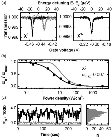
Figure 1. (a) Differential transmission of the neutral exciton (left) and singly charged exciton (right) in a single self-assembled quantum dot. (b) The differential absorption at resonance plotted against laser power. The solid black line is the result expected for a two-level system. The solid grey line models the power dependence of an absorbing system including an intermediate shelving state. (c) Left: The differential absorption signal as a function of time at zero detuning (black) and several linewidths away from the exciton resonance (grey); right: Histogram of the differential absorption amplitude signal at zero detuning.
- A. Högele et al., Phys. Rev. Lett. 93, 217401 (2004).
- B. Alén et al., Appl. Phys. Lett. 83, 2235 (2003); A. Högele et al., Physica E 21, 175 (2004).
NEMS
Nanoelectromechanical systems (NEMS) are both fascinating as objects for fundamental studies of electromechanical coupling on the nanoscale and promising for a large variety of applications like extremely sensitive sensors and actuators. A still unsolved problem is how to easily excite nanomechanical elements and control their motion. Although on a micromechanical scale we have performed experiments on tuning the mechanics of microlevers with light and even a light-induced cooling of the microlever has been achieved. This opens new routes for driving and controlling nanomechanical systems by optical means. NEMS devices carved out of Silicon on insulator (SOI) have either been built in form of vertical nano-pillars or in form of laterally defined beams, the latter optionally with a hole-aperture through the whole substrate beneath the nanostructures. Vertical nano-pillars loaded by an excess charge have been shown to oscillate if driven by Coulomb forces. Laterally defined nanobeams with no substrate beneath have been shown to provoke images of high clarity in a scanning confocal optical microscope.
Cavity cooling of a microlever
Constanze Höhberger-Metzger and Khaled Karrai
The prospect of realizing entangled quantum states between macroscopic objects and photons has recently stimulated interest in new laser-cooling schemes. For example, laser-cooling of the vibrational modes of a mirror can be achieved by subjecting it to a radiation or photothermal pressure, actively controlled through a servo loop adjusted to oppose its brownian thermal motion within a preset frequency window. In contrast, atoms can be laser-cooled passively without such active feedback, because their random motion is intrinsically damped through their interaction with radiation. We reported [1] direct experimental evidence for passive (or intrinsic) optical cooling of a micromechanical resonator. We exploit cavity-induced photothermal pressure to quench the Brownian vibrational fluctuations of a gold-coated silicon microlever from room temperature down to an effective temperature of 18 K (Fig. 1). Extending this method to optical-cavity-induced radiation pressure might enable the quantum limit to be attained, opening the way for experimental investigations of macroscopic quantum superposition states involving numbers of atoms of the order of 1014.
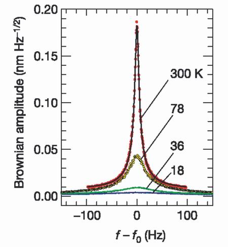
Figure 1. Cavity-induced cooling of the lever vibrational resonance. Brownian (thermal) motion amplitude spectra of the lever vibrational resonance measured for four different laser power levels. The largest peak spectrum data (dots) centered on 7 280 Hz was obtained at 80 nW. The full line is the calculated Brownian (i.e. thermal) noise spectrum using a temperature T = 300 K. Increasing the laser power in three steps to 130mW reduced markedly the area of the peak and shifted its frequency to 7 300 Hz. The calculated spectra fit perfectly the data obtained at three different increasing laser powers when effective temperatures T = 78, 36 and 18 K are assumed.
- C. Höhberger-Metzger and K. Karrai, Nature 432, 1002 (2004)
Easy operation and enhanced electronic functionality of nanoelectromechanical systems
Dominik V. Scheible and Jörg P. Kotthaus, in cooperation with Robert H. Blick and Christoph Weiss
As mechanical systems at the nanometer scale broaden their role in experimental physics and electronic engineering, concepts of easy operation and manufacturing become more and more important. In a vertical nanoelectromechanical system (NEMS) we have demonstrated a straightforward method for mechanical excitation with frequencies approaching the GHz-domain [1]. As shown in Fig. 1, a silicon nano-pillar can oscillate between two facing gates, driven by the Coulomb force exerted onto the excess charge being present on the top gold island (I). With this device, both operation and the manufacturing of the device itself have been successfully demonstrated in a greatly simplified manner. Furthermore, we have observed field emission from the gold island of a similar NEMS device [2]. The electrical isolation of the emitter yields new I-V-characteristics in this case, compared to the classic linear Fowler-Nordheim description (see Fig. 2). The mechanical degree of freedom of the nanoscale pendulum nevertheless allows for continuous operation and field emission is exploited to enhance the current to the regime of nanoamperes, the latter being accessible by conventional electronics.
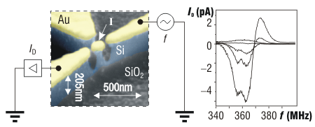
Figure 1. The vertical nanomechanical electron pendulum and its spectral current close to the fundamental resonance at approx. 370 MHz.
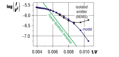
Figure 2. Linear Fowler-Nordheim current as compared to the I-V-characteristics of an electrically isolated emitter, mounted on a nanomechanical pendulum.
- D. V. Scheible and R. H. Blick, Appl. Phys. Lett. 84, 4632 (2004).
- D. V. Scheible, C. Weiss, J. P. Kotthaus, and R. H. Blick, Phys. Rev. Lett. 93, 186801 (2004).
Optical imaging of freely suspended nanoelectromechanical systems with no substrate beneath
Christine Meyer, Heribert Lorenz, and Khaled Karrai, in cooperation with Omar Sqalli
Caused by their small sizes and their even smaller actuation ranges the deflections of freely suspended nanocantilevers are not easy to investigate. Indirect methods like measuring the reflected radio frequency power bear some doubts in interpretation while means of direct investigation like SEM imaging may destructively interfere with the sample. Far field optical imaging instead is a non-invasive tool but (at least in the visible spectrum) is not capable of resolving most NEMS due to the Abbé diffraction limit. Additionally, the interference with the light reflected from the substrate that normally is located in close vicinity to usual nanostructures makes the resulting images hard to interpretate [1]. A removal of the substrate beneath the nanostructure in this sense not only enhances the image contrast but also eliminates its parasitic electrostatical influence. The imaging of such NEMS with a hole-aperture beneath as shown in Fig. 1 has been shown to yield very clear images (see Fig. 2) [2].
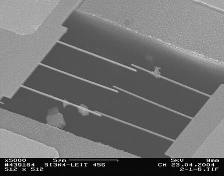
Figure 1. SEM image of a NEMS consisting of six 10 µm long and 200 nm wide cantilevered beams with a hole-aperture beneath them that reaches through the whole substrate (oblique view). Every two cantilevers in a pair oppose each other with a distance of about 200 nm between them.
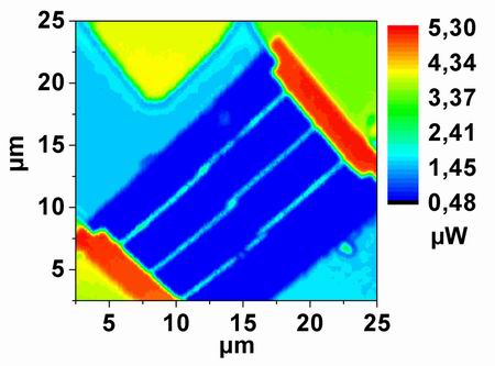
Figure 2. Scanning confocal optical image of the structure shown in Fig. 1 using an imaging wavelength of 635 nm and a slip-stick positioner (attocube systems AG) in step-scan mode for imaging (top view).
- C. Meyer, H. Lorenz, and K.Karrai, Appl. Phys. Lett. 83, 2420 (2003).
- C. Meyer, O. Sqalli, H. Lorenz, and K. Karrai, Proceedings of the IEEE 4th Conference on Nanotechnology, 435 (2004).
Nanodevices and bio-templated nanostructures
Surface acoustic wave (SAW) devices utilizing “nanoquakes” for chemical sensors and microfluidic actuators continue to be one aspect of our research though this effort is increasingly shifting to the new group of Achim Wixforth at the University of Augsburg. In a cooperation with the group of Thomas Bein at the chemistry department of LMU and the Advalytix AG we are studying chemical gas sensors employing nanoporous films as selective absorbers and sensing the gas absorption via the modified propagation of SAW in a delay line. In cooperation with Advalytix SAW devices are successfully employed for microfluidics both as pumps and as fluidic sensors aiming towards lab-on-a-chip applications. Another fruitful lab-on-a-chip oriented project has been continued with the young start-up Nanion in the area of improving patch-clamp techniques. Here single ion channel recordings have been successfully performed on a glass chip developed in this cooperation. Whereas the above projects aim at employing solid state device techniques for biomedical applications we are also happy to host the Emmy-Noether young investigator group of Fritz Simmel which is using biophysical and bioinspired techniques to create new electronic and mechanical functions in a bottom-up approach. To this end, the unique molecular recognition properties of DNA molecules are utilized to build complex supramolecular networks or to direct the synthesis of functional materials, but also to construct artificial molecular machines. For example, DNA could be shown to be able to direct the synthesis of chains of copper sulfide nanoparticles, in bulk a semiconducting compound. In another project, an artificial molecular device based on a DNA aptamer was developed with the functionality of a “molecular hand”.
Contacting Gold Nanoparticles with Carbon Nanotubes by Self-Assembly
Tobias Smorodin, Christian J.-F. Dupraz, Udo Beierlein, Jörg P. Kotthaus
Carbon nanotubes (CNTs) are unique nanostructures with fascinating electrical, mechanical, chemical and optical properties. One of the challenges in the use of CNTs is the difficulty to manipulate them, e.g. for positioning, attachment to electrodes, controlled modification of their properties, etc. One of the most promising ways to overcome these problems is by chemical modification, taking advantage of the molecular properties of CNTs. By following this route, we functionalized single-wall carbon nanotubes (SWNTs) with biotin at the ends and side-walls of the nanotubes in a series of chemical reactions. Streptavidin-coated gold nanoparticles were attached to the biotin-modified SWNTs in solution in a self-assembly process. Gold nanoparticles which connected two SWNTs were selected and contacted for transport measurements (Fig. 1). At low temperatures, Coulomb blockade oscillations were observed as a function of gate voltage. The size of the nanoparticles can be enlarged by catalytic deposition of gold leading to current increase through the SWNT-nanoparticle-SWNT junction (Fig. 2). In another experiment, thiolized SWNTs were prepared and selectively attached to gold electrodes.
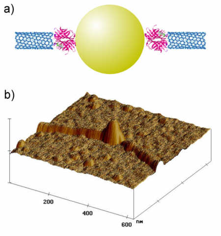
Figure 1. (a) Schematic representation of two SWNTs attached to a gold nanoparticle via streptavidin. (b) AFM image of such a SWNT-nanoparticle-SWNT junction.
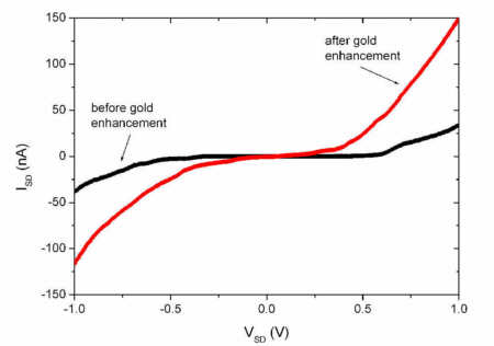
Figure 2. Variation of the current with source-drain voltage for a CNT-nanoparticle-CNT system at T = 4.2 K before (black curve) and after (red curve) catalytic deposition of gold.
DNA-templated materials synthesis
Patrick Nickels, Wendy U. Dittmer, Stefan Beyer, Jörg P. Kotthaus, Friedrich C. Simmel
Continuing our efforts to template electronically functional materials by DNA (as already reported last year), we synthesized and characterized polyaniline nanowires along DNA. To this end, DNA was incubated in a low pH solution of aniline to attach positively charged anilinium ions along the negatively charged DNA backbone. The aniline monomers were subsequently polymerized using various methods: Oxidative polymerization by horseradish peroxidase (HRP) in the presence of hydrogen peroxide, oxidative polymerization using ammonium persulfate and photooxidative polymerization using ruthenium bipyridinium complexes under blue light illumination. All three methods lead to the formation of polyaniline domains along the DNA, as evidenced by AFM (Fig. 1) and spectroscopic analysis. Only wires synthesized by the latter two methods, however, were amenable to conduction measurements (Fig. 2).
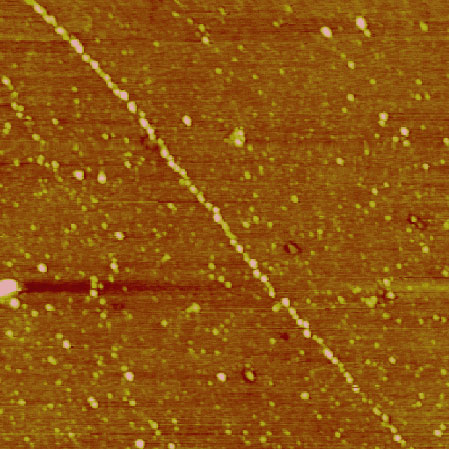
Figure 1. AFM image of polyaniline templated on stretched DNA from bacteriophage λ.
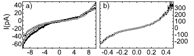
Figure 2. I-V curve obtained on a network of DNA-polyaniline nanowires synthesiuzed by the HRP/peroxide method deposited between gold electrodes with a spacing of a) 1 µm and b) 100 nm.
- P. Nickels, W. U. Dittmer, S. Beyer, J. P. Kotthaus, and F. C. Simmel, "Polyaniline nanowire synthesis templated by DNA", Nanotechnology 15, 1524-1529 (2004).
Molecular machinery
Wendy U. Dittmer, Friedrich C. Simmel
One of the chief goals of molecular nanoscience is the creation of autonomous nanodevices which can perform useful tasks, e.g. aid in transport and self-assembly of nanoobjects in analogy to processes controlled by the molecular machinery found in living cells. To perform complex tasks without interaction with an external operator, however, it is necessary to somehow "program" a series of operational steps into the nanodevices themselves. In the case of DNA nanomachines, a programming language is readily at hand: The genetic code. We therefore attempted to encode instructions for nanomechanical DNA devices into artificial genes. As a first step towards this goal we demonstrated that a DNA code containing a promotor sequence for T7 RNA polymerase can be used to control the closing of the previously introduced DNA "tweezers" (Fig. 1).
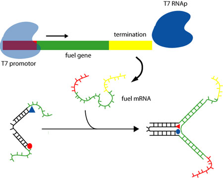
Figure 1. Schematic depiction of closing of DNA tweezers controlled by mRNA: An artificial gene contains a promotor sequence for T7 RNA polymerase, the instructions for closing (fuel gene) and a termination sequence.
- W. U. Dittmer and F. C. Simmel, "Transcriptional control of DNA-based nanomachines", Nano Letters 4, 689-691 (2004).
Soft lithographic cell patterning
Tim Liedl, Friedrich C. Simmel in cooperation with Wolfgang Parak
In this project, soft lithographic methods for the controlled deposition of live cells were established in our group and - combined with semiconductor nanoparticle labeling - used for differential cell motility experiments.
Master stamps were fabricated using optical lithography and the high-aspect ratio negative resist SU8-50. From these masters replicas were molded using the elastomeric material poly(dimethylsiloxane) (PDMS). With these PDMS stamps patterns of alternating hydrophobicity could be generated on glass and silicon surfaces, e.g. by the localized formation of molecular monolayers octadecyltrichlorosilane (OTS). Cell preferentially adhere to more hydrophilic areas and therefore attach to the negative of a hydrophobic pattern (Fig. 1). Using water soluble fluorescent semiconductor nanocrystals with two distinct fluorescence emission wavelengths, we differentially labeled two different cell lines. The cells were put on a hydrophobic gradient pattern on which cells with differing adherence properties migrate at different speeds (Fig. 2).
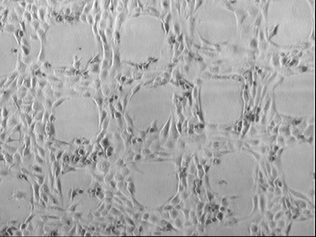
Figure 1. MDA-MB 235s breast cancer cells spread on a glass slide with squares made hydrophobic with OTS by PDMS stamping.
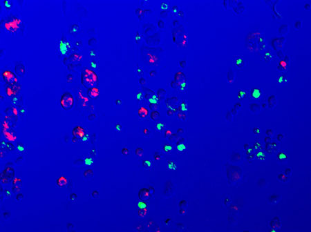
Figure 2. Breast cancer cells from two different cell lines labeled with green and red fluorescing quantum dots on a hydrophobic/hydrophilic stripe gradient pattern stamped on a glass surface.
Diploma theses completed in 2004
- Daniel König
"Nano-elektromechanische Transistoren" - Felix Schöfer
"Electron-Phonon-Wechselwirkung in niedrigdimensionalen Halbleiter-Heterostrukturen" - Michael Lambacher
"Elektronischer Transport durch molekulare Leiter" - Patrick Nickels
"Elektronische Eigenschaften von DNA-basierten Nanodrähten" - Martin Kroner
"Spektroskopie an einzelnen ladungsdurchstimmbaren selbstorganisierten Halbleiter-Quantenpunkten" - Clemens Rössler
"Kopplung und Manipulation von Elektronenspinzuständen in elektrostatisch definierten Quantenpunkten" - Ulrike Holz
"Optisch durchstimmbare Dynamik von nanomechanischen Systemen"
PhD theses completed in 2004
- Florian Beil
"Akustische Hochfrequenzanregung von Nanoresonatoren auf Halbleiterbasis" - Christian Schulhauser
"Elektronische Quantenpunktzustände induziert durch Photonemission" - Christine Meyer
"Untersuchung von elektrostatisch betätigten Nanostellelemanten" - Dominik Scheible
"Integration elektronischer Funktionalität in nanomechanische Systeme" - Michael Sztucki
"The use of Synchrotron Radiation to study Overgrowth Phenomena in InAs/ GaAs Nanostructures"
Guest scientists in 2004
- Professor Dr. Valeri Dolgopolov,
Russian Academy of Sciences, Chernogolovka, Alexander von Humboldt Stiftung - Professor Dr. Mansour Shayegan,
Princeton University, USA, Alexander von Humboldt Stiftung - Dr. Richard Warburton,
Heriot-Watt University, Edinburgh, UK, SFB 631 - Dr. Vadim Khrapay,
Russian Academy of Sciences, Chernogolovka, Alexander von Humboldt Stiftung - Prof. Alexander O. Govorov,
Russian Academy of Sciences, Novosibirsk, and Ohio University, Volkswagen Stiftung - Prof. Jim Allen,
University of California, Santa Barbara, USA, Alexander von Humboldt Stiftung - Hyun Seok,
University of Wisconsin, Madison, USA - Dr. Carla Abilio,
Fundacào papa a Ciència e Tecnologia, Ministèry for Science and Technology, Portugal - Dr. Wendy Dittmer (neé Huynh), University of California, Berkeley, USA, Alexander von Humboldt Stiftung
Group members in 2004
Senior scientists
- Prof. Jörg P. Kotthaus
- Prof. Khaled Karraï
- Dr. Udo Beierlein
- Dr. Heribert Lorenz
- Dr. Stefan Ludwig
- Dr. Friedrich Simmel
- Dr. Eva Weig
Secretary
- Martina Jüttner
Technical staff
- Hans-Peter Kiermaier
- Wolfgang Kurpas
- Stephan Manus
- Alexander Paul
- Stefan Schöffberger
Ph.D. students
- Florian W. Beil
- Stefan Beyer
- Florian Bickel
- Christian Dupraz
- Andreas Gärtner
- Stephan de Haan
- Alexander Högele
- Constanze Höhberger
- Andreas K. Hüttel
- Tim Liedl
- Daniel König
- Martin Kroner
- Christine Meyer
- Alexander Müller
- Andreas Reuter
- Clemens Rössler
- Dominik V. Scheible
- Daniel Schröer
- Christian Schulhauser
- Christoph Strobl
- Markus Vogel
Diploma students
- Matthias Fiebig
- Eike Friedrichs
- Ulrike Holz
- Ulrich Hoyer
- Martin Kroner
- Michael Lambacher
- Patrick Nickels
- Sebastian Remi
- Clemens Rössler
- Tobias Smorodin
Publications in 2004
- K. Karrai, R. J. Warburton, C. Schulhauser, A. Högele, B. Urbaszek, E.J. McGhee, A. Govorov, J. M. Garcia, B. D. Gerardot, and P. M. Petroff
"Hybridization of electronic states in quantum dots through photon emission"
Nature 427, 135-138 (2004) - E. M. Weig, R. H. Blick, T. Brandes, J. Kirschbaum, W. Wegscheider, M. Bichler, and J. P. Kotthaus
"Single-Electron-Phonon Interaction in a Suspended Quantum Dot Phonon Cavity"
Phys. Rev. Lett. 92, 046804-1-4 (2004) - S. de Haan, A. Lorke, J. P. Kotthaus, W. Wegscheider, and M. Bichler
"Rectification in Mesoscopic Systems with Broken Symmetry: Quasiclassical Ballistic Versus Classical Transport"
Phys. Rev. Lett. 92, 056806-1 -4 (2004) - A. Högele, B. Alen, F. Bickel, R. J. Warburton, P. M. Petroff, and K. Karrai
"Exciton fine structure splitting of single InGaAs self-assembled quantum dots"
Physica E 21, 175 - 179 (2004) - Wendy U. Dittmer and Friedrich C. Simmel
"Transcriptional Control of DNA-Based Nanomachines"
Nano Letters 4, 689 - 691 (2004) - Dominik V. Scheible, and Robert H. Blick
"Silicon nanopillars for mechanical single-electron transport"
App. Phys. Lett. 84, 4632 - 4634 (2004) - H. Qin, A. W. Holleitner, A. K. Hüttel, R. H. Blick, W. Wegscheider, M. Bichler, K. Eberl, and J. P. Kotthaus
"Probing coherent electronic states in double quantum dots"
Phys. Stat. Sol. (c) 1, 2094 - 2110 (2004) - B. Urbaszek, E. J. McGhee, M. Krüger, R. J. Warburton, K. Karrai, T. Amand, B. D. Gerardot, P. M. Petroff, and J. M. Garcia
"Temperature-dependent linewidth of charged excitons in semiconductor quantum dots: Strongly broadened ground state transitions due to acoustic phonon scattering"
Phys. Rev. Lett. 69, 035304-1 -6 (2004) - Alexander V. Chaplik, and Robert H. Blick
"On geometric potentials in quantum-electromechanical circuits"
New Journal of Physics. 6, 33 (2004) - S. de Haan, A. Lorke, J. P. Kotthaus, M. Bichler, and W. Wegscheider
"Quantized transport in ballistic rectifiers: sign reversal and step-like output"
Physica E 21, 916 - 920 (2004) - A. O. Govorov, K. Karrai, R. J. Warburton, A. V. Kalameitsev
"Charged excitons in quantum dots: novel magnetic behavoir and Auger processes"
Physica E 20, 295 - 299 (2004) - B. Alèn, K. Karrai, R. J. Warburton, F. Bickel, P. M. Petroff, J. Martinez-Pastor
"Absorption spectroscopy of single InAs self-assembled quantum dots"
Physica E 21, 395 - 399 (2004) - C. Schulhauser, R. J. Warburton, A. Högele, A. O. Govorov, K. Karrai, J. M. Garcia, B. D. Gerardot, P. M. Petroff
"Emission from neutral and charged excitons in a single quantum dot in a magnetic field"
Physica E 21, 184 - 188 (2004) - Christine Meyer, Heribert Lorenz, Khaled Karrai
"Electroluminescence from a current-emitting nanostructured silicon device"
Superlattices and Microstructures 33, 339 - 346 (2004) - Christian J.-Fr. Dupraz, Patrick Nickels, Udo Beierlein, Wendy U. Huynh, Friedrich C. Simmel
"Towards molecular-scale electronics and biomolecular self-assembly"
Superlattices and Microstructures 33, 369 - 379 (2004) - Robert H. Blick, and Dominik V. Scheible
"A quantum electromechanical device: the electromechanical single-electron pillar"
Superlattices and Microstructures 33, 397 - 403 (2004) - Khaled Karrai, and Richard J. Warburton
"Optical transmission and reflection spectroscopy of single quantum dots"
Superlattices and Microstructures 33, 311 - 337 (2004) - Robert H. Blick, and Dominik V. Scheible
"Nano-Electromechanical Transistor operated as a Bi-Polar Current Switch"
Nanotechnology, 4th IEEE Conference 2004, 258 - 259 (2004) - F. W. Beil, R. H. Blick, and A. Wixforth
"Standing acoustic waves imaged by a nanomechanical resonator"
Physica E 21, 1106 - 1110 (2004) - A. K. Hüttel, J. Weber, A. W. Holleitner, D. Weinmann, K. Eberl, and R. H. Blick
"Nuclear spin relaxation probed by a single quantum dot"
Phys. Rev. B 69, 073302-1 - 4 (2004) - Daniel R. Koenig, Dominik V. Scheible, and Robert H. Blick
"Drastic enhancement of nanoelectromechanical-system fabrication yield using electron-beam deposition"
Appl. Phys. Lett. 85, 157 - 159 (2004) - Wendy U. Dittmer, Andreas Reuter, and Friedrich C. Simmel
"A DNA-Based Machine That can Cyclically Bind and Release Thrombin"
Angew. Chemie 43, 3549 - 3553 (2004) - Dominik V. Scheible, Christoph Weiss, and Robert H. Blick
"Effects of low attenuation in a nanomechanical electron shuttle"
J. Appl. Phys. 96, 1757-1759 (2004) - Wendy U. Dittmer, and Friedrich C. Simmel
"Chains of semiconductor nanoparticles templated on DNA"
App. Phys. Lett. 85, 633 - 635 (2004) - Patrick Nickels, Wendy U. Dittmer, Stefan Beyer, Jörg P. Kotthaus
"Polyaniline nanowire synthesis templated by DNA"
Nanotechnology 15, 1524-1529 (2004) - C. J. Strobl, C. Schäflein, U. Beierlein, J. Ebbecke, and A. Wixforth
"Carbon nanotube alignment by surface acoustic waves"
Appl. Phys. Lett. 85, 1427 -1429 (2004) - D.V. Scheible, C.Weiss, J. P. Kotthaus, and R. H. Blick
"Periodic Field Emission from an Isolated Nanoscale Electron Island"
Phys. Rev. Lett. 93, 186801-1 - -4 (2004) - Alexander Högele, Stefan Seidl, Martin Kroner, Khaled Karrai, Richard J. Warburton,
Brian D. Gerardot, and Pierre M. Petroff
"Voltage-Controlled Optics of a Quantum Dot"
Phys. Rev. Lett. 93, 217401-1 - -4 (2004) - Constanze Höhberger-Metzger and Khaled Karrai
"Cavity cooling of a microlever"
Nature 432, 1002 - 1005 (2004) - J. Ebbecke, C. J. Strobl, and A. Wixforth
"Acoustoelectric current transport through single-walled carbon nanotubes"
Phys. Rev. B 70, 233401-1 - -4 (2004) - C. J. Strobl, Z. Guttenberg, and A. Wixforth
"Nano- and Pico-Dispensing of Fluids on Planar Substrates Using SAW"
IEEE transactions on ultrasonics, ferroelectrics, and frequency control, 1432 1-5 (2004) - J. Krauß, J. P. Kotthaus, A. Wixforth, M. Hanson, D. C. Driscoll, A. C. Gossard, D. Schuh, and M. Bichler
"Capture and release of photonic images in a quantum well"
Appl. Phys. Lett 85, 5830 - 5832 (2004) - A. Wixforth, C. Strobl, Ch. Gauer, A. Toegl, J. Scriba, and Z. v. Guttenberg
"Acoustic Manipulation of Small Droplets"
Annal. Bioanal. Chem 379, 982 - 991 (2004) - A. W. Holleitner, A. Chudnovskiy, D. Pfannkuche, K. Eberl, and R. H. Blick
"Pseudospin Kondo correlations versus hybridized molecular states in double quantum dots"
Phys. Rev. B 70, 075204 - -5 (2004) - F.C. Simmel and B. Yurke
"DNA-based nanodevices"
Encyclopedia of Nanoscience and Nanotechnology, Ed. H.S. Nalwa, American Scientific Publishers, Stevenson Ranch (2004) - Michael Lambacher, Christian J.-F. Dupraz, Udo Beierlein, Jörg P.Kotthaus, Ulrich S.
Schubert, Philip R. Andres
"Device for conductance measurements of molecular systems"
Nanotechnology, 4th IEEE Conference 2004, 515 - 517 (2004)
Invited talks in 2004
Khaled Karrai
- "Hybridization of electronic states in quantum dots through photon emission"
New Developments in Solid State Physics, Mauterndorf, Austria, Febuary 2004 - "Optical spectroscopy on single charge-tunable semiconductor quantum dot"
2004 China-Germany Workshop on Semiconductor Nanostructure Physics and Devices, Beijing, China, February/March 2004 - "Hybridization of electronic states in quantum dots through photon emission"
QD 2004, 3rd Int. Conf. on Quantum dots, Banff, Canada, May 2004 - "Hybridization of electronic states in quantum dots through photon emission"
Physics of Semiconducting Compounds, Jaszowiec 2004 - "Optical spectroscopy on single charge-tunable semiconductor quantum dot"
Monte Verità Summer School on Semiconductor Quantum Dots: Physics and devices, Monteverità, Ascona, Switzerland, September 2004 - "Optical Tunable Mechanics of Microlevers"
7th Int. Conf. on Non-contact Atomic Force Microscopy, Seattle, USA September 2004 - "Voltage-controlled optics of a single quantum dot"
Quantum Information Processing, Herrsching, September 2004 - "Laser cooling of microlevers"
Nanoscience: linking disciplines, Venice International University, September/October 2004
Jörg P. Kotthaus
- "Ballistic Rectification with Quasi 1-D Channels in GaAs"
March Meeting of the American Physical Society, Montreal, March 2004 - "Quantum Phenomena in Nanoelectromechanical Systems"
Int. Symposium on "Quantum Hall Systems and Quantum Materials", University of Hamburg, Hamburg, September 2004 - "Some Quantum Phenomena in Nano-Electro-Mechanical Systems"
CIAR Nanoelectronics Workshop, Vancouver, November 2004 - "Nano-Elektromechanik auf Silizium"
11. Siltronic-Silicium-Symposium, Siltronic AG, Ising, Germany, November 2004 - "Perspektiven der Nanowelt - Abbild versus Illustration"
Symposium "Das Bild der Wissenschaft", Freie Universität Berlin mit VolkswagenStiftung, Dezember 2004
Friedrich Simmel
- "Patch clamp on a chip"
Edgar-Lüscher-Seminar, Serneus, Februar 2004 - "DNA nanodevices"
WE-Heraeus seminar on "Nanophysics of DNA", Bad Honnef, März 2004 - "DNA devices based on aptamers"
Conference on "Foundations of Nanoscience", Snowbird, Utah, April 2004 - "Biomolecular nanoscience"
Summer school of the Int. Max Planck Research School devoted to the theme "Nanomaterials - Science and Engineering", Stuttgart, April 2004 - "DNA nanostructures and nanodevices"
5th International Wilhelm and Else Heraeus Summer School: "Molecules: Building blocks for future nanoelectronics", Wittenberg, August 2004, - "DNA-based molecular machines and devices"
Nanoroadmap conference, "Present situation and forecasts of nanotechnology in: Materials, health and medical systems, energy", Rom, November 2004 - "DNA-based machines and devices"
5th Int. EMBL PhD students symposium: "Design of Life - learning from nature", Heidelberg, Dezember 2004
Eva Weig
- "Single electron tunneling and phonon quantum confinement in
freely suspended quantum dots"
1st Workshop on Arrays of Quantum Dots and Josephson Junctions, European Science Foundation, Medena, Kroatia, October 2004 - "Effects of phonon quantum confinement in freely suspended quantum dots"
11th Advanced Heterostructure Workshop, Hawaii, USA, December 2004
Senior scientists of cooperating groups
- Gerhard Abstreiter, Max Bichler, Dieter Schuh
Walter Schottky Institut, TU München, Germany. - S. James Allen
University of California, Santa Barbara, USA. - Thomas Bein
CeNS, LMU München, Germany. - Robert Blick
University of Wisconsin-Madison, USA. - Tobias Brandes
University of Manchester, England. - Alik Chaplik
Institute of Semiconductor Physics, Novosibirsk, Russia. - Valeri Dolgopolov
Russian Academy of Sciences, Chernogolovka, Russia. - Karl Eberl
Max-Planck-Institut für Festkörperforschung, Stuttgart, Germany. - Jochen Feldmann
CeNS, LMU München, Germany. - Jorge M. Garcia
Instituto de Microelectronica de Madrid, Spain. - Hermann Gaub, Wolfgang Parak
CeNS, LMU München, Germany. - Arther C. Gossard
Materials Department, University of California - Santa Barbara, USA. - Alexander O. Govorov
Institute of Semiconductor Physics, Novosibirsk, Russia, and Ohio University, USA - Robert D. Grober
Department of Applied Physics, Yale University, USA. - Reinhard Guckenberger
MPI of Biochemistry, Martinsried, Germany. - Wolfgang Heckl
CeNS, LMU München, Germany. - Serge Huant
Laboratoire de Spectrométrie Physique, Université Joseph Fourier Grenoble and CNRS, France. - Paul Leiderer
University of Konstanz, Germany. - Axel Lorke
Universität Duisburg-Essen, Germany. - Hartmut Metzger
ESRF Grenoble, France. - Karl Neumeier
Walther-Meissner-Institut für Tieftemperaturforschung, Germany. - Lukas Novotny
The Institute of Optics, University of Rochester, USA. - Pierre M. Petroff
University of California - Santa Barbara, USA. - Joachim Rädler, Bert Nickel
LMU München, Germany. - Mansour Shayegan
Princeton University, USA. - Klaus H. Schmidt, Ulrich Kunze
Werkstoffe der Elektrotechnik, Ruhr-Universität Bochum, Germany. - Ulrich Schubert
Eindhoven University of Technology, Dutch Polymer Institute, Eindhoven, Netherlands - Sergio E. Ulloa
Ohio University, Athens, USA - Richard Warburton
Heriot-Watt University, Edinburgh, U.K. - Werner Wegscheider, Christoph Strunk Institut für Angewandte und Experimentelle Physik, Universität Regensburg, Germany.
- Daniel van der Weide
University of Wisconsin-Madison, USA. - Dietmar Weinmann
Institut de Physique et Chimie des Matériaux de Strasbourg, France. - Andreas Wieck
Ruhr-Universität Bochum, Germany. - Christoph Weiss
C. v. Ossietzky Universität Oldenburg, Germany. - Achim Wixforth
Universität Augsburg, Germany.
Financial support in 2004
Funding of this work via the following agencies is gratefully acknowledged: