

Research report 2009
- Introduction
- Electronic properties
- Characterization of an electrostatically defined Si/SiGe Double Quantum Dot
- Phonon-mediated vs. Coulombic Back-Action in Quantum Dot circuits
- Phonon-mediated non-equilibrium interaction between mesoscopic devices
- An electron avalanche amplifier in a two-dimensional electron system
- Asymmetric non-linear response of the integer quantum Hall effect
- Optical and optoelectronical phenomena in nanodevices
- Nanomechanical systems
- Fluctuating nanomechanical system in a high finesse optical microcavity
- Near-field cavity optomechanics with nanomechanical resonators
- Increasing the charging energy of a nano-mechanical electron shuttle
- Dielectric transduction of nanomechanical motion
- Stroboscopic Down-Conversion of Nanomechanical Motion
- On-chip interferometric detection of nanomechanical motion
- Bachelor theses in 2009
- Diploma theses in 2009
- PhD theses in 2009
- Guest scientists in 2009
- Group members in 2009
- Publications in 2009
- Invited talks in 2009
- Senior scientists of cooperating groups
- Financial support in 2009
Introduction
Nanoscale devices and systems continue to be the major objects of our research. In our laboratory we realize devices employing top-down techniques derived from semiconductor processing, sometimes complemented with bottom-up assembly via chemical and biochemical routes. Our research aims at both, a deeper fundamental understanding of physical behavior in the nanometer regime and the realization of novel devices, functions, and systems utilizing a variety of nanotechnologies.
Nanoelectronic quantum transport studied at low temperatures is a major research subject and in part embedded in the DFG-funded SFB 631 “Solid-State Based Quantum Information Processing”. Here Stefan Ludwig is now leading our efforts on better understanding electronic transport properties through nanoscale devices fabricated out of GaAs- as well as Si-based heterostructures. Optical quantum control of GaAs-based quantum dots and carbon nanotubes is the major research theme of the newly formed nano-photonics group lead by Alexander Högele. This is complemented by our efforts to study the emission and absorption of excitonic ensembles confined in two or three dimensions, which aims at a better understanding of excitonic interactions, possibly ultimately leading to Bose-Einstein condensation. Our research on Nano-Electro-Mechanical Systems (NEMS), lead by Eva Weig and myself, has recently been substantially expanded by introducing new methods of actuation and detection of resonant nanomechanical motion via electrical and optical near-fields and by studying their linear and non-linear behavior. Since fall 2009 we also participate in the collaborative European project “Quantum Nano-Electro-Mechanical Systems” (QNEMS) coordinated by TU Delft.
In all of our research we profit from stimulating interactions with colleagues within the “Nanosystems Initiative Munich” (NIM) and the Center for NanoScience (CeNS) and former members of our group who continue to fruitfully interact with us, in particular Alexander Holleitner and Friedrich Simmel, both now at TU Munich, Khaled Karrai at attocube and now also a honorary professor at LMU, Richard Warburton at Heriot-Watt University in Edinburgh and Sasha Govorov at Ohio University in Athens, USA. New stimulus also comes with extended stays of former and present Humboldt awardees and postdoctoral fellows, such as Valeri Dolgopolov of the Russian Academy of Sciences in Chernogolovka, Katarzyna Kowalik from the Grenoble High Field Laboratory, and Ivan Favero, now at Université Paris Diderot. Being embedded in both national and international collaborations provides additional stimulus to our research.
We were happy to provide 8 highly motivated physics students the opportunity to complete their Bachelor theses in our group, which they seemed to enjoy after two years of heavy and sometimes frustratingly formal course loads that came with the rather bureaucratic and less creativity stimulating transition from the traditional Diploma to the new Bachelor/Master degree system. With the successful completion of 5 one-year diploma thesis and 3 doctoral thesis projects our labs were densely populated which has also been a challenge to all thesis supervisors. Our publication activity reflects an intermediate dip in the more advanced research personnel with 17 publications well below our annual average but this is at least partially compensated by quite a few publications with high impact, as reflected in both the journals of their appearance, their mention in the relevant press and the numerous invitations of members of our group to major international conferences and workshops. Most importantly, all young students and scientists that left our group after completing their respective research projects were able to get attractive professional positions in spite of the general economic turn-down, a fact that makes us confident that our educational efforts remain quite successful.
As in previous years it is my special pleasure to thank all members of our group for their continued enthusiasm and excellent research and I wish those that have left us in 2009 all the best for their new careers. I also gratefully acknowledge the continuous generous support by our funding agencies. We hope that many readers worldwide enjoy this report and we are happy to receive any feedback.
Munich, May 25, 2010
Jörg P. Kotthaus
Electronic properties
Reducing the length scales of transistors well below 100 nanometers is one of the present key efforts in semiconductor industry. At the same time such tiny structures allow the observation of phenomena obeying the fundamental laws of quantum mechanics. In our clean room we fabricate a variety of gate-controlled devices by e-beam lithography starting from GaAs/AlGaAs heterostructures that contain a two-dimensional electron system (2DES). The gates lying on the sample surface can be voltage biased in order locally deplete the 2DES. This technique allows us to further structure the 2DES and for instance create tunnel coupled zero-dimensional quantum dots or artificial molecules. In 2009 we have extended our efforts towards quantum computing within a close collaboration with Dominique Bougeard and Gerhard Abstreiter at the Walter Schottky Institute, TU-München, to a new material system, namely heterostructures made from silicon and germanium. It promises longer spin-coherence times compared to the mature GaAs based devices, because of the possibility to get rid of nuclear spins. In addition we have continued to study back-action of a quantum point contact detector onto coupled quantum dots, which could be used as quantum bits. In 2009 we managed to experimentally separate different contributions to back-action, mediated by phonons vs. Coulomb interaction. In order to prove the importance of phonons for the interaction between mesoscopic circuits a separate experiment has been performed in addition. It turns out that also electron-electron scattering in the leads of a biased quantum point contact influences back-action. We have therefore set up an experiment to study it. In addition to gaining informations about the electron-electron scattering length far from equilibrium we were able to build an avalanche electron amplifier in this device. Finally, in 2009 we have investigated the breakdown behavior of the integer quantized Hall effect in narrow gate defined high mobility Hall bars. The results go beyond the well established Landauer-Büttiker edge channel picture and support an emerging theory based on the screening by Coulomb interaction between the electrons in the 2DES.
Characterization of an electrostatically defined Si/SiGe Double Quantum Dot
Andreas Wild, Jürgen Sailer, Gerhard Abstreiter,
Dominique Bougeard and Stefan Ludwig,
in collaboration with Kohei M. Itoh and Eugene E. Haller
The Silicon-Germanium (Si-Ge) material system is a promising approach towards electron spin based quantum information processing in scalable electrostatically defined quantum dot (QD) architectures. Si is expected to have outstanding spin coherence properties compared to the well studied III-V material system due to small hyperfine interaction which can also be reduced by isotopic purification, weak spin-orbit interaction and the absence of piezoelectric coupling.
We demonstrated the successful realization of a Si-based double quantum dot with a nearby single dot that was employed as a charge detector with a sensitivity of about 0.1 fractional electron charges as shown in figure 1.
Stable operation or e.g. tuning the interdot tunnel coupling of our device in the presence of unintentional charge noise was possible as exemplarily illustrated in the charge stability diagrams of figure 2. This allowed us to study our device in various regimes from open to closed tunnel barriers to the leads. In the latter one, the electrons in the double dot are isolated such that only interdot transitions are possible.
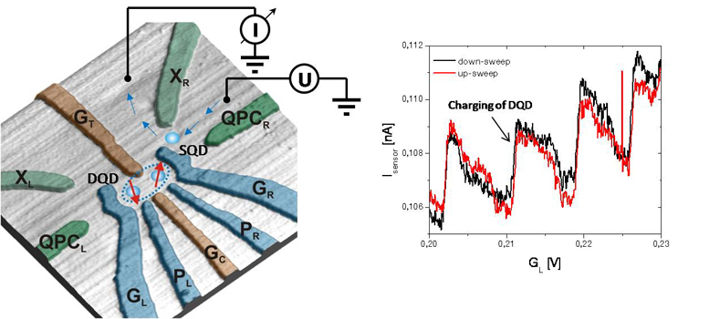
Figure 1. AFM image of a double quantum dot device (DQD). The nearby single quantum dot (SQD) which is used as a charge detector shows a strong response to a varying occupation of the double dot.
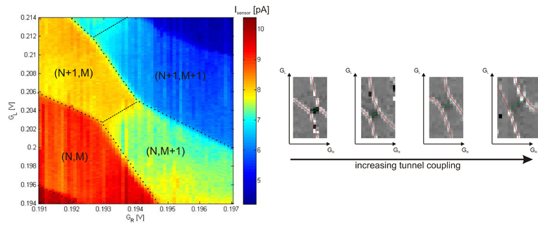
Figure 2. (Left) Current through charge sensor as a function of both plunger gate voltages of the double dot. Such a color coded charge stability plot depicts the various occupation states in the vicinity of a triple point region where two charge states become energetically degenerate. (Right) Numerical derivative of a charge stability plot in a triple point region demonstrating the tuneability of the interdot tunnel coupling by gate voltages.
Phonon-mediated vs. Coulombic Back-Action in Quantum Dot circuits
Daniel Harbusch, Daniela Taubert and Stefan Ludwig,
in collaboration with Hans Peter Tranitz and Werner Wegscheider
Coupled quantum dots (QDs) are promising candidates for applications as qubits in solid state quantum information processing schemes. Here we perform charge spectroscopy on an electrostatically defined double QD (gate layout in Fig. 1a). A voltage VQPC is applied across a quantum point contact (QPC-I in Fig. 1a) and the linear response of the current through the QPC to a modulation of another voltage applied to gate β is measured. This so-called transconductance is plotted in Figs. 1b and 1c as a function of two gate voltages Vβ and Vγ. The transconductance reaches extremal values whenever the charge in at least one of the QDs changes by one electron. As a result we find the charging lines of both QDs (dark), along which the charge in one QD fluctuates by one electron. Along the charge reconfiguration lines (white double lines) one electron tunnels between the two QDs. In addition we observe triangular-shaped regions which indicate specific non-equilibrium charge occupations of the QDs. The size of these triangles increase with VQPC. Hence, we identify the QPC detector as energy source that causes the non-equilibrium charge occupations. In detail, the biased QPC emits non-equilibrium charge carriers into its leads which then relax via electron-electron interaction, the emission of plasmons, or acoustic phonons. Partial reabsorption of the emitted energy can result in charge fluctuations in (coupled) QDs and thereby causes indirect back-action [1,2,3]. The detailed positions of the triangles, their shapes and additional features (for instance the stripes) allow us to sort out the contributions of phonon-mediated versus coulombic back action and to identify the relevant relaxation channels within the double QD.
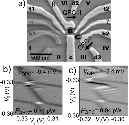
Figure 1. (a) Scanning electron microscope picture of the sample surface. It shows gold gates used to electrostatically define QDs and QPCs. Darker gates are not used. (b,c) Stability diagrams of the double QD for two different voltages applied across the QPC.
- D. Taubert, M. Pioro-Ladriere, D. Schröer, D. Harbusch, A. S. Sachrajda, and S. Ludwig, Phys. Rev. Lett. 100, 176805 (2008)
- D. Harbusch, D. Taubert, H. P. Tranitz, W. Wegscheider, and S. Ludwig, arXiv:0910.4093 (2009)
- G. J. Schinner, H. P. Tranitz, W. Wegscheider, J. P. Kotthaus, and S. Ludwig, Phys. Rev. Lett. 102, 186801 (2009)
Phonon-mediated non-equilibrium interaction between mesoscopic devices
Georg J. Schinner, Jörg P. Kotthaus and Stefan Ludwig
in collaboration with Hans Peter Tranitz and Werner Wegscheider
Quantum interactions in nanoscale circuits become increasingly important with shrinking device dimensions. In mesoscopic circuits interactions can be transmitted by Coulomb interaction, by plasmons or by phonons. Here, we investigate the contribution of acoustic phonons to the non-equilibrium interaction between electrically separated circuits at low temperatures (~0.1 K). The left figure shows a Hall-bar (elevated), which contains a two-dimensional electron system (2DES). Negative voltages applied to the (colored) metal gates cause local depletion of the 2DES. They are adjusted to define a quantum point contact (QPC) and potential barriers (B1 and B3). B1 is very high and electrically separates the emitter (left of B1) from the detector circuit (right of B1). By biasing the almost pinched-off QPC with the voltage VSD ballistic electrons are injected with a well defined excess energy (eVSD) into the emitter circuit (compare sketch). While B1 is opaque for electrons energy can still be transmitted into the unbiased detector circuit, for example by acoustic phonons. These energy-quanta can then excite electrons from the cold Fermi-sea (sketch). Barrier B3 in the detector circuit is tuned to have a height near the Fermi-energy so that it locally separates excited electrons from the now positively charged remaining Fermi-sea. Because most energy is absorbed between barriers B1 and B3 the energy selectivity of barrier B3 results in a detector current I3. The color scale plot shows the detector current as a function of the voltage VSD applied across the QPC and the height of barrier B3 compared to the Fermi energy EF. We observe a sudden onset (dashed line) of the detector current at a barrier height of 1.3 meV above the Fermi-energy. Hence the excess energy of electrons in the detector circuit is limited by an upper bound of about 1.3 meV. This value corresponds to the maximum energy of acoustic phonons that can be absorbed by equilibrium electrons and indicates that the energy is indeed transmitted by phonons rather than Coulomb interaction [1]. Our studies illustrate the importance of acoustic phonons for the interaction in mesoscopic circuits.
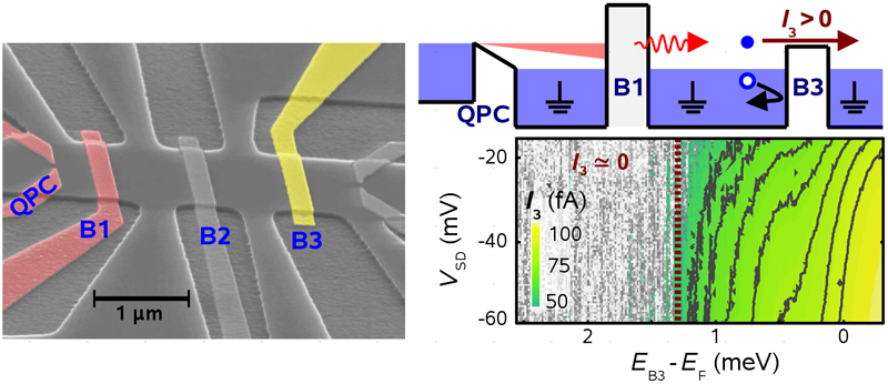
Figure 1.
- G. J. Schinner, H. P. Tranitz, W. Wegscheider, J. P. Kotthaus, and S. Ludwig, Phys. Rev. Lett. 102, 186801 (2009)
An electron avalanche amplifier in a two-dimensional electron system
Daniela Taubert, Georg Schinner and Stefan Ludwig,
in collaboration with Hans Peter Tranitz, Werner Wegscheider, Constantin Tomaras and Stefan Kehrein
Ballistic transport of electrons far from equilibrium is investigated in a
cold two-dimensional electron system. We observe interaction of excited
charge carriers with a degenerate Fermi sea in a three-terminal device
shown in Figure (a) [1]. The side and collector (C) contacts are grounded
while a negative voltage VE is applied to the emitter contact (E).
Electrons are injected with a well-defined energy across the almost
pinched-off quantum point contact (BE). They transfer momentum and energy to
cold electrons in the Fermi sea by electron-electron scattering. This can be
interpreted as the excitation of electron-hole pairs, with holes being missing
electrons in the Fermi sea of the conduction band. The additional barrier BC
between the grounded side and collector contacts is used to separate the
excited electrons from the holes (Figure (c)).
Electrons supplied from the grounded side contact neutralize the holes.
As a result, the collector current exceeds the emitted current IC > IE, and the side current Iside
becomes negative. The observed amplification ratio α = IC / IE is shown in
Figure (b) as a function of VE and the voltage VBC applied to the barrier
gate. The top axis depicts the barrier height with respect to the Fermi
energy EF. The amplification effect depends on the energy of the injected
electrons, the emitter current IE, and the height of the barrier used for
separating electrons and holes. Our experiments provide detailed
information about the electron-electron scattering dynamics in a ballistic
system far from equilibrium. A preliminary model based on numerical
calculations using a random phase approximation is in agreement with our
data.
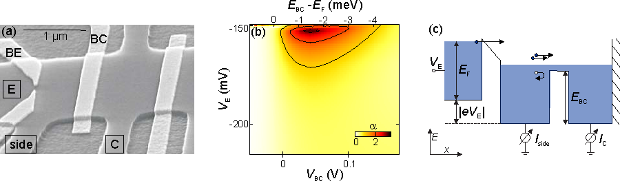
Figure 1. (a) Electron micrograph of the sample. The elevated area contains a two-dimensional electron system. Top gates (light gray) are used to define electrostatic barriers BE and BC. Ohmic contacts “E”, “side”, and “C” are marked. (b) Current amplification ratio α = IC / IE, plotted against barrier voltage VBC and bias VE. Contour lines show α = 1,2,3. (c) Energy diagram sketching the experiment.
- D. Taubert, G. J. Schinner, H. P. Tranitz, W. Wegscheider, C. Tomaras, S. Kehrein, and S. Ludwig, arXiv:1001.5201 (2009)
Asymmetric non-linear response of the integer quantum Hall effect
Jose Horas, Dawid Kupidura and Stefan Ludwig,
in collaboration with Afif Siddiki and Werner Wegscheider
The integer quantum Hall effect (IQHE) is one of the most studied phenomena in two-dimensional electron systems. Its main features (quantized plateaus of the Hall resistance and periodically vanishing longitudinal resistance) are well explained within the Landauer-Büttiker edge channel picture for linear response measurements. An emerging screening theory of the IQHE [1] considers the detailed confinement potential and the influence of Coulomb interaction between the electrons. In contrast to the established models it makes predictions beyond linear response, for instance in the regime in which a large applied current destroys the IQHE. Here, we investigate an asymmetric breakdown of the IQHE as a function of the current value and its direction in conjunction with an asymmetric lateral confinement potential defining the Hall bar. Our electrostatic definition of the Hall bar via Schottky-gates (Fig. 1a) allows a systematic control of the steepness of the confinement potential at the edges of the Hall bar. The more negative the voltage applied to a gate is the harder will the corresponding edge of the Hall-bar be. A softer edge (flatter confinement potential) results in more stable Hall plateaus and a breakdown at a larger current density. The main result of this research is shown in Fig. 1b [2]. It plots the Hall resistance RH as a function of a magnetic field (applied perpendicular to the Hall bar) for four different situations regarding the current direction and hard vs. soft edges of the Hall bar. For one soft and one hard edge the breakdown current clearly depends on the current direction, resembling rectification. This non-linear magneto-transport effect confirms the predictions of the screening theory of the IQHE [1].
Figure 1. (a) Scanning electron microscope picture of the sample surface. Four gold top gates (light gray) are biased with negative voltages in order to define the Hall bar within the two-dimensional electron system, which resides 110 nm below the surface of this GaAs/AlGaAs heterocrystal. A current is driven through the Hall-bar between the ohmic contacts (not shown) at S (source) and D (drain). A perpendicular magnetic field and the resulting Landauer-Büttiker edge channels are indicated in red. (b) Hall resistance as a function of magnetic field for four different situations.
- A. Siddiki and R. R. Gerhardts, Phys. Rev. B 70, 195335 (2004).
- A. Siddiki, J. Horas, D. Kupidura, W. Wegscheider, and S. Ludwig, arXiv:0911.4832 (2009)
Optical and optoelectronical phenomena in nanodevices
Optical studies of exciton spin memory in coupled quantum wells were performed by K. Kowalik-Seidl, X. P. Vögele and B. Rimpfl. The experiments showed efficient polarization conservation indicating long spin relaxation times of indirect excitons when excited quasi-resonantly through the direct excitonic states. J. T. Glückert successfully established sample fabrication techniques for the study of single optically active carbon nanotubes. He further demonstrated the functionality of the cryogenic photoluminescence setup by recording spectra and local maps of nanotube emission at liquid nitrogen temperatures. P. Paulitschke and J. Rieger studied effects of enhanced photoluminescence from silicon nitride photonic crystal nanocavities that were fabricated by collaborators N. Nüsse and B. Löchel at the Helmholtz-Zentrum Berlin. Their findings point toward novel experiments with hybrid opto-mechanical systems.
Optical studies of exciton spin memory in coupled quantum wells
K. Kowalik-Seidl, X. P. Vögele, B. Rimpfl, S. Manus and J. P. Kotthaus,
in collaboration with D. Schuh and A.W. Holleitner
Semiconductor heterostructures with tunable spatial separation of electrons and holes attract a great attention for their possible applications in optoelectronic devices. Recent experiments performed on coupled quantum wells (CQWs) have reported exciton spin transport over several micrometers, demonstrating indirectly a long exciton spin relaxation [2]. We have investigated the spin memory of indirect excitons in GaAs/AlGaAs coupled quantum wells via time resolved and polarization sensitive photoluminescence (PL).
In order to precisely define the initial spin polarization of excitons we optimized the process of resonant excitation. We took advantage of the quasi-resonant excitation into direct exciton states, which has proven to be very efficient in similar structures [2]. We have measured the degree of circular polarization (CP) for the indirect exciton emission while tuning systematically the excitation wavelength in the range 780-790nm, enabling us to drive the excitation energy through the direct excitonic states (see Fig.1). For non-resonant excitation no significant polarization of indirect excitons PL has been measured, whereas a clear enhancement of the circular polarization was observed for the quasi-resonant excitation conditions. The maximum value of CP was about 55%. Such efficient polarization conservation suggests a long relaxation time of the exciton spin, which exceeds the radiative recombination time. To confirm this hypothesis, time resolved photoluminescence spectra were recorded. We observed that the indirect exciton emission remained circularly polarized several tens of nanosecond after the laser pulse. Our findings from continuous and time-resolved experiments directly demonstrated the long spin relaxation for indirect excitons in CQWs.
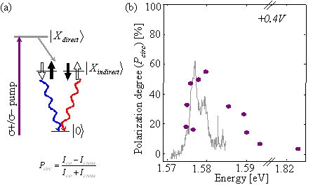
Figure 1. (a) Energy level diagram of the experiment. (b) Polarization degree of the indirect excitons as a function of the laser energy (purple points). Spectra of the direct exciton line are shown in grey.
- S. Zimmermann, A. Wixforth, J. P. Kotthaus, W. Wegscheider, and M. Bichler, Science 283, 1292 (1999).
- J. R. Leonard, Y. Y. Kuznetsova, Sen Yang, L. V. Butov, T. Ostatnick, A. Kavokin and A. C. Gossard, Nano Lett., published online (2009).
Low-temperature photoluminescence from individual single-wall carbon nanotubes
J. T. Glückert and A. Högele
The quantum nature of the photoluminescence emission from semiconducting single-wall carbon nanotubes (CNTs) has been reported recently [1]. The results represent the first step towards quantum optical control of exciton and spin states in photoactive semiconducting CNTs. Photoluminescence spectroscopy is used as a main tool to study optical excitations in individual nanotubes at low-temperatures. To this end we have established methods for sample fabrication and analysis. It is crucial to isolate individual nanotubes on samples with a low density of CNTs. Figure 1 (a) shows an AFM image of a single nanotube on Si/Si02 substrate with an average diameter of 0.65 nm - a characteristic feature of CoMoCat single-wall carbon nanotube material. We have further built up a cryogenic spectroscopy setup and characterized its performance by detecting CNT photoluminescence at liquid nitrogen temperatures. A representative optical map of a low-density sample is presented in Figure 1 (c) and shows locally isolated emission patterns which can be assigned to individual CNTs.
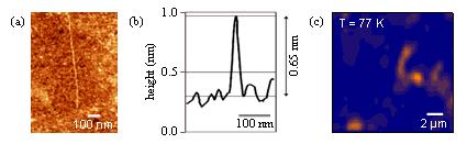
Figure 1. AFM image of a single carbon nanotube on Si02 substrate with a length of 600 nm (a) and an average diameter of 0.65 nm (b). Using a confocal cryogenic microscopy setup and exciting the photoluminescence in a sub-micron spot we recorded the map in (c) by laterally scanning the sample that was cooled to liquid nitrogen temperature of 77 K. The false color image features localized maxima of photoluminescence from individual semiconducting carbon nanotubes (bright orange spots).
- A. Högele, C. Galland, M. Winger, and A. Imamoglu, Phys. Rev. Lett. 100, 217401 (2008).
Observation of enhanced photoluminescence from silicon nitride photonic crystal nanocavities
P. Paulitschke, J. Rieger, J. P. Kotthaus and E. M. Weig,
in collaboration with N. Nüsse and B. Löchel (Helmholtz-Zentrum Berlin)
Photonic crystal resonators have attracted much attention over recent years, since they open innovative ways to control light, including the stopping and the trapping of light, quantum information processing and the enhancement of light-matter interactions, as well as the coupling of a mechanical degree of freedom to a nanocavity. This potential is expected to lead to a wide range of applications for integrated on-chip photonics. We investigate two dimensional silicon nitride (SiN) photonic crystal nanocavities (Fig.1, left panel) with resonance wavelengths in the visible range. The intrinsic photoluminescence (PL) of the SiN between 500-750 nm is used as an internal light source to excite the cavity modes. The luminescence was detected with a home-built confocal microscope. We observe a significant enhancement of PL and studied the resonance wavelength, the quality factor and polarization properties of the cavity modes (Fig.1, right panel).
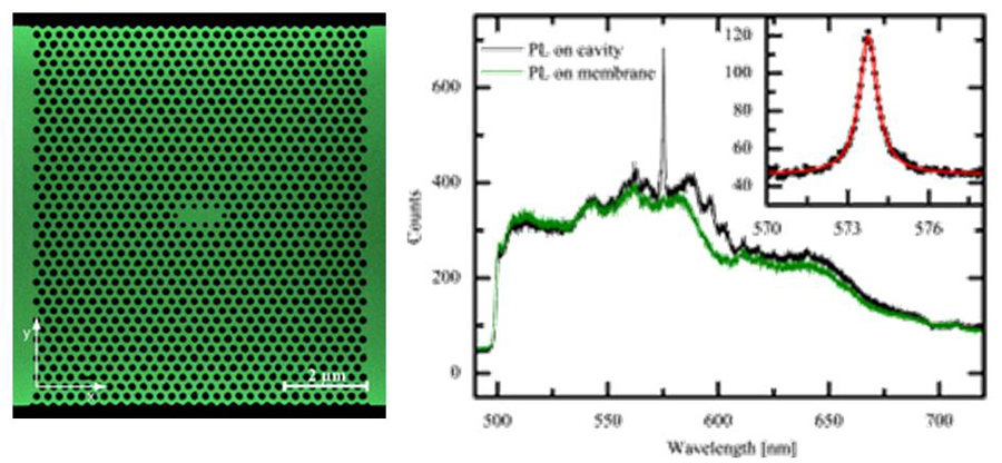
Figure 1. Left panel: False colored SEM image of a photonic crystal cavity with three missing holes (L3 cavity) in a SiN membrane. Right panel: Luminescence spectra of a SiN L3 membrane on and off the cavity excited with a blue diode laser. The inset shows a Lorentzian fit to the cavity resonance peak.
Nanomechanical systems
Nanomechanical systems are freely suspended nanostructures with nanoscale cross-sections and lengths of up to several 10 microns. We investigate the resonant mechanical properties of these nano-oscillators, as well as their coupling to optical or electronic systems. While optomechanical coupling has been well-known in macro- and microscale mechanical systems such as gravitational wave detectors or AFM levers, the field of cavity nano-optomechanics has only recently taken stage. However, it can be shown that the resulting absorptive or dispersive interaction based on photon-induced forces gives rise to a highly sensitive readout of the position fluctuations of the resonator as well as to interesting back-action effects. An example for nano-electromechanical coupling is the nanomechanical charge shuttle, where mechanically induced electron transport near the Coulomb blockade regime is investigated. The above examples are enabled by a good control of the basic resonator properties, including both intrinsic properties such as dissipation, as well as external conditions such as the employed transduction schemes. Therefore, the efficient actuation as well as the sensitive readout of nanomechanical motion have been a further core topic of our research.
Fluctuating nanomechanical system in a high finesse optical microcavity
S. Stapfner, P. Paulitschke, H. Lorenz and E. M. Weig,
in collaboration with Ivan Favero (Paris Diderot), David Hunger (LMU), Jakob Reichel (ENS) and Khaled Karrai (LMU)
The idea of extending cavity quantum electrodynamics experiments to sub-wavelength sized nanomechanical systems has been recently proposed in the context of optical cavity cooling and optomechanics of deformable cavities. We have developed an experiment involving a single nanorod consisting of about 109 atoms hosted by a silicon lever precisely positioned into the confined mode of a miniature high finesse Fabry-Perot microcavity [1]. The experimental setup is depicted in Fig. 1. The optical transmission of the cavity is affected not only by the static position of the nanorod but also by its vibrational fluctuation (Fig. 2). The Brownian motion of the nanorod is resolved with a displacement sensitivity of 200 fm/√Hz at room temperature. Besides a broad range of sensing applications, cavity-induced manipulation of optomechanical nanosystems and back-action are anticipated.
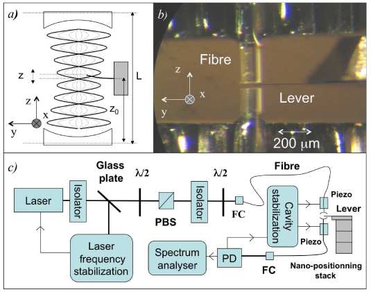
Figure 1. Nanorod vibrating in the microcavity resonantly probed by a laser. a) Schematics of nanorod at position z0 in the microcavity and vibrating with an amplitude z. b) Optical micrograph of the host silicon lever plunged between the two fibre end-facets in order to position the nanorod in the cavity mode. c) Set-up schematics (PBS: polarizing beam splitter, FC: fibre coupler, PD: photodiode).
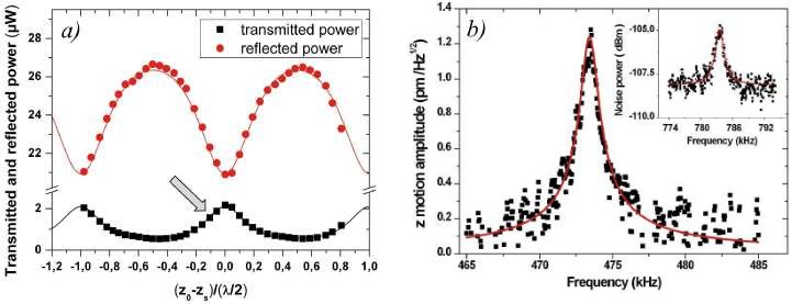
Figure 2. Perturbation of the cavity transmission by the nanorod. a) Optical power transmitted and reflected by the cavity at resonance as a function of the nanorod base position z0 normalized to the laser wavelength λ (zs being the average position of the lever, roughly in the middle of the cavity). The arrow indicates the operating point of maximum gradient dT/dz0. b) Brownian motion amplitude spectrum z for the first flexural resonance of the nanorod. Inset: Transmission noise power spectrum around the frequency of the second flexural resonance of the nanorod, for a resolution bandwidth of 300 Hz of the spectrum analyzer.
- Favero I., Stapfner S., Hunger D., Paulitschke P., Reichel J., Lorenz H., Weig E. M., Karrai K., Optics Express 17, 12813 (2009).
Near-field cavity optomechanics with nanomechanical resonators
Q. P. Unterreithmeier, E. M. Weig and J. P. Kotthaus,
in collaboration with G. Anetsberger, O. Arcizet, R. Rivière, A. Schliesser and T. J. Kippenberg (Max-Planck Institute for Quantum Optics)
Cavity-enhanced radiation-pressure coupling between optical and mechanical degrees of freedom allows quantum-limited position measurements and gives rise to dynamical back-action, enabling amplification and cooling of mechanical motion. We have demonstrated purely dispersive coupling of high-Q nanomechanical resonator fabricated from high stress silicon nitride to an ultrahigh-finesse optical microcavity realized by a silica microtoroid. Upon approaching the two systems, the resonator enters the evanescent field of the cavity, which gives rise to a pronounced cavity frequency shift while leaving the cavity linewidth unaffected (Fig. 1). The Brownian position fluctuations of the resonator can be read out via the optical cavity transmission (Fig. 2). Due to the high Q and small mass of the nanomechanical resonator, as well as the large cavity finesse, a displacement sensitivity of 580 am/√Hz is achieved, which is below the resonator's expected zero-point fluctuations of 820 am/√Hz. Apart from the first demonstration of quantum-limited displacement sensing of a nanomechanical resonator, dynamical back-action mediated by the optical dipole force has been observed, leading to laser-like coherent nanomechanical oscillations solely induced by radiation pressure [1].
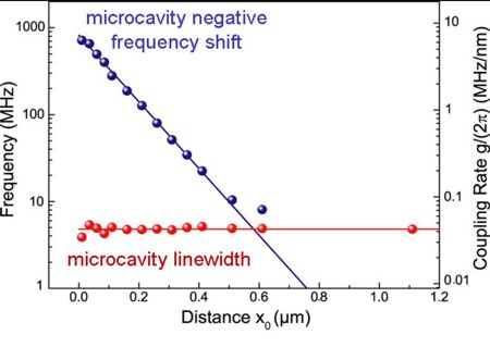
Figure 1. Negative optical frequency shift (blue) and linewidth (red) of a 58 μm diameter microtoroid cavity as a function of the distance to a doubly clamped silicon nitride string with dimensions 110 nm x 800 nm x 25 μm. The data reveal purely dispersive coupling without introducing a measurable degradation of the microcavity's optical decay rate.
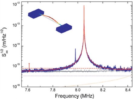
Figure 2. Room-temperature Brownian noise of the nanomechanical resonator with a fundamental resonance frequency of 8 MHz (inset). For an optical input power of 65 μW, the displacement imprecision reaches a value of 570 am/√Hz (grey line), which is 0.7 times the standard quantum limit, that is, the oscillator's expected zero-point fluctuations (red dashed line).
- Anetsberger G., Arcizet O., Unterreithmeier Q. P., Rivière R., Schliesser A., Weig E. M., Kotthaus J. P., and Kippenberg T. J., Nature Physics 5, 909 (2009).
Increasing the charging energy of a nano-mechanical electron shuttle
D. R. König, S. Weber, J. P. Kotthaus and E. M. Weig
Since its prediction in 1998, mechanical single electron transport by means of a nanomechanical charge shuttle operated in the Coulomb blockade regime has been a major goal [1]. We investigate a shuttle system consisting of a nanoscale gold island situated in the center of a doubly clamped, freely suspended, 14 μm long nanoresonator fabricated from high stress silicon nitride. A set of customized weights attached to each resonator enables frequency multiplexing in large arrays of nominally identical resonators. Each resonator can oscillate between a set of source and drain electrodes placed on either side of the island, allowing for the observation of a shuttling current in case the resonator is vibrating with sufficient amplitude.
While stable and reproducible charge transport has been recently realized in the quasi-ohmic high temperature regime [2], Coulomb blockade limited single electron shuttling is yet to be demonstrated. This is related to a set of opposing requirements: While nanomechanical motion with large amplitudes is required to move the island to within a tunnelling distance of either electrode by means of non-electrical actuation to avoid cross-talk, low temperatures have to be maintained to resolve Coulomb blockade for a given island geometry. The pathway to the Coulomb blockade regime thus involves a continuous downscaling of the island capacitance which gives rise to an increasing charging energy. We have realized a miniaturized shuttle with island dimensions of L = 176 nm, B = 52 nm and H = 30 nm (Fig. 1). This corresponds to a shuttle capacitance of 13.4 aF, which should allow to resolve Coulomb blockade at 4.2 K.
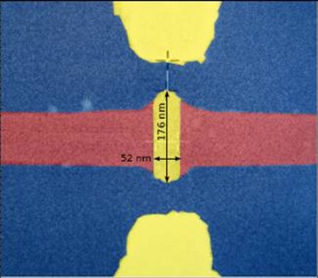
Figure 1. (a) A false-colour scanning electron microscope (SEM) micrograph of the central region of a miniature nanomechanical electron shuttle, displaying the gold island and electrodes (yellow) as well as the center of the silicon nitride resonator (red).
- Gorelik L.Y. et al., Phys. Rev. Lett. 80, 4526 (1998).
- Koenig D. R., Weig E. M., and Kotthaus J. P., Nature Nanotechnology 3, 482 (2008).
Dielectric transduction of nanomechanical motion
Q. P. Unterreithmeier, E. M. Weig and J. P. Kotthaus
In a recent work [1] we investigated the applicability of dielectric forces to actuate nanomechanical systems. Any polarizable object placed in a non-uniform electric field is attracted towards regions of higher field intensity. In our setup the electric field is created by two suitably biased gold electrodes placed nearby the oscillating mechanical element, see Fig. 1. A key feature is that the mechanical element is thereby not modified; in particular no metal has to be deposited on top of the resonator.
Applying a DC voltage influences a dipolar moment within the resonator such that an additional RF voltage modulates the attractive force, thus causing resonant motion of the mechanical oscillator (Fig. 2). The actuation shows to be very effective; e.g. one can achieve forces that are a factor of 106 larger than the weight of the element. The scheme can be applied to any material and works over a wide range of actuation frequencies. Moreover, the fact that the resonator moves in a gradient force field allows simple voltage tuning of its resonance frequency, as seen in Fig. 2c.
Finally, it was demonstrated that the capacitive influence of the moving resonator on the gold electrodes can be used to detect the resonant motion. An ongoing project aims at an enhancement of the achieved detection sensitivity.
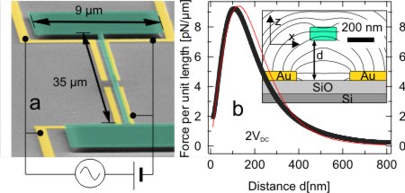
Figure 1. a) Setup and b) dielectric force per length vs. vertical distance d.
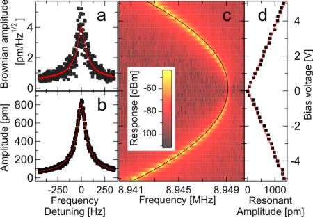
Figure 2. Response of an a) thermally and b)-d) dielectrically actuated nanomechanical resonator at room temperature.
- Unterreithmeier Q. P., Weig E. M., and Kotthaus J. P., Nature 458, 1001 (2009).
Stroboscopic down-conversion of nanomechanical motion
Q. P. Unterreithmeier, S. Manus and J. P. Kotthaus
A common detection scheme of nanomechanical motion is to illuminate the beam and collect the reflected signal. Because of interference and scattering, one obtains an intensity modulation with displacement that is detected with a photodiode. However, any photodiode is a compromise on the one hand of amplification factor and on the other hand bandwidth (i. e. response time) and noise. To overcome this limitation, we introduce a modulation of the incoming laser beam that is slightly detuned from the mechanical oscillation frequency. Thereby, the reflected intensity contains a part oscillating on this detuning frequency. In a recent work [1], we are able to employ this technique to detect the various mechanical resonances of a 35 micron long doubly clamped nanoresonator fabricated from high stress SiN up to frequencies of 60 MHz using a detector with a bandwidth of 1 MHz. The obtained set of frequencies allows us to conclude that our nanoresonator behaves like an elastic string rather than a rigid beam. We utilize this finding to introduce an amplitude conversion factor to convert the measured signal into absolute displacement.
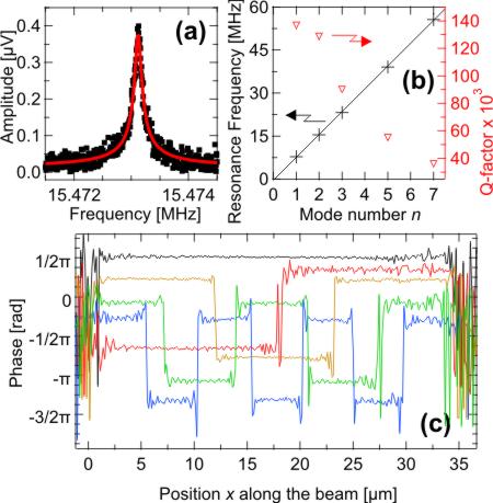
Figure 1. a) Typical frequency response of a driven mechanical oscillator. b) Frequency and quality factor of the measured resonances. c) Phase distribution of the various resonances measured along the beam.
- Unterreithmeier Q. P., Manus S., and Kotthaus J. P., Appl. Phys. Lett. 94, 263104 (2009).
On-chip interferometric detection of nanomechanical motion
Q. P. Unterreithmeier, T. Faust, S. Manus and J. P. Kotthaus
In this project, an integrable on-chip displacement detection of nanomechanical motion is developed [1]. Creating a gold/silicon Schottky contact close to the silicon nitride resonator allows the measurement of the mechanical resonant motion through the local modulation of the optical near-field intensity and a thereby modulated photocurrent (Fig. 1a-c). This scheme poses no restrictions on resonator material and avoids additional damping as it would be caused by beam metallization typical for other detection schemes. The achieved sensitivity of 1 pm/√Hz enables the detection of the Brownian motion of our mechanical resonators at room temperature (Fig. 1d).
In addition, we demonstrate self-oscillation, by implementing a feedback scheme that utilizes a recently developed dielectric actuation scheme [2]. The natural linewidth of the mechanical resonance can thus be lowered by a factor of 8 (Fig. 2), making the system more responsive, an important aspect for sensing applications. We thereby achieve a highly integrable, all electrical on-chip transduction.
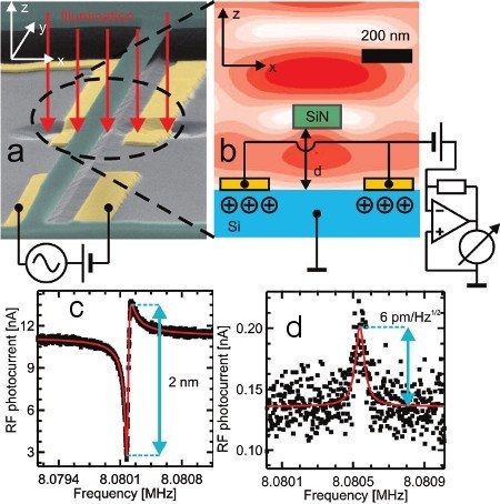
Figure 1. a) SEM micrograph and b) schematic of the setup, showing the (simulated) light intensity around the resonator. c) Driven response of the resonator, the Lorentzian lineshape is distorted by capacitive crosstalk. d) Measurement of the Brownian motion of the resonator, allowing to determine the sensitivity of the detection.
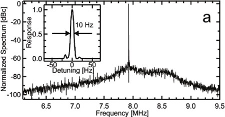
Figure 2. Output signal of the NEMS oscillator realized with the on-chip detection. The peak corresponds to the mechanical resonance, its narrow linewidth displayed in the inset.
- Unterreithmeier Q. P., Faust T., Manus S., and Kotthaus J. P., Nanoletters DOI:10.1021/nl903556s (advance online publication, 2010).
- Unterreithmeier Q. P., Weig E. M., and Kotthaus J. P., Nature 458, 1001 (2009).
Bachelor theses completed in 2009
- Maximilian Brunner
“Die Auswirkungen von Thermospannungen auf Transportmessungen bei tiefen Temperaturen” - Daniel Burchardt
“Entwicklung und Charakterisierung eines Tieftemperaturprobenhalters für hochfrequente Messungen an Nanostrukturen” - Christian Ecke
“Nano-mechanischer Elektronentransport mit Gleichspannungsantrieb” - Dario Hügel
“Dissipation in Nanoelectromechanical Systems” - Lizhe Liu
“Polarisationsaufgelöste Messungen an Exzitonen in gekoppelten Quantentöpfen” - Patrik Loch
“FDTD Simulationen von photonischen Kristallkavitäten mit intgriertem nano-mechanischem Resonator” - Benjamin Michaelis
“Fabrikation und Untersuchen von geschlitzten Substraten für zugspannungsabhängige Messungen” - Simon Weber
“Nano-mechanischer Einzel-Elektronen-Transport im Coulombblockade-Regime”
Diploma theses completed in 2009
- Thomas Faust
“Nanomechanik zugverspannter Siliziumnitridresonatoren. Integrierte Detektion, Rückkopplung, Realisierung eines Speichers, Dämpfungsmechanismen” - Johannes Mösl
“Transportspektroskopie an Quantenpunkten in Nanodrähten” - Johannes Rieger
“Towards integrated nano-optomechanical systems with photonic crystal cavities” - Florian Seilmeier
“Magnetfeldabhängigkeit indirekter Exzitonen in GaAs/AlGaAs-Quantentöpfen” - Sebastian Stapfner
“Kavitätsoptomechanik im Subwellenlängenbereich”
PhD theses completed in 2009
- Klaus-Dieter Hof
“Optisch induzierter Ladungstransport in mesoskopischen Halbleitersystemen” - Dawid Kupidura
“Spinwechselwirkung eines Doppelquantenpunkts mit dem Kernfeld. Anpassschaltung für einen rf-Quantenpunktkontakt” - Bernd Zebli
“Optoelektronische Sensibilisierung von Kohlenstoffnanoröhrchen durch CdTe-Nanokristalle”
Guest scientists in 2009
- Prof. Alexander Holleitner
Technische Universität München, Walter Schottky Institut - Prof. Friedrich Simmel
Technische Universität München - Prof. Alexander O. Govorov
Ohio University, Athens, OH, USA, SFB 631 - Prof. Valeri Dolgopolov
Russian Academy of Sciences, Chernogolovka, Russia, Alexander von Humboldt Stiftung - Dr. Katarzyna Kowalik
Grenoble High Magnetic Field Laboratory, Grenoble, France, Alexander von Humboldt Stiftung
Group members in 2009
Senior scientists
- Prof. Jörg P. Kotthaus
- Prof. Alexander Högele
- Dr. Heribert Lorenz
- Dr. Stefan Ludwig
- Dr. Eva-Maria Weig
- Dr. Daniel König
- Dr. Felix Mendoza
- Dr. Constanze Metzger
Secretary
- Martina Jüttner
Technical staff
- Philipp Altpeter
- Hans-Peter Kiermaier
- Wolfgang Kurpas
- Stephan Manus
- Reinhold Rath
Ph.D. students
- Thomas Faust
- Matthias Fiebig
- Jan Tibor Glückert
- Daniel Harbusch
- Klaus-Dieter Hof
- Dawid Kupidura
- Philipp Paulitschke
- Gunnar Petersen
- Johannes Rieger
- Georg Schinner
- Florian Seilmeier
- Sebastian Stapfner
- Daniela Taubert
- Xaver Vögele
- Quirin Unterreithmeier
- Bernd Zebli
Diploma students
- Matthias Benecke
- Max Empl
- Thomas Faust
- Matthias Hofmann
- Johannes Mösl
- Lukas Ost
- Johannes Rieger
- Bernhard Rimpfl
- Enrico Schubert
- Florian Seilmeier
- Norbert Seltner
- Sebastian Stapfner
Publications in 2009
- J. Sailer, V. Lang, G. Abstreiter, G. Tsuchiya, K. M. Itoh, J. W. Ager, E. E. Haller, D. Kupidura, D. Harbusch, S. Ludwig, and D. Bougeard
“A Schottky top-gated two-dimensional electron system in a nuclear spin free Si/SiGe heterostructure”
Phys. Status Solidi RRL 3, No.2, 61-63 (2009). - M. Fiebig, C. Erlen, M. Göllner, P. Lugli and B. Nickel
“Spatially resolved photoresponse measurements on pentacene thin-film transistors”
Appl. Phys. A, 95, 113-117 - T. L. Sobey, S. Renner and F. C. Simmel
“Assembly and melting of DNA nanotubes from single-sequence tiles”
J. Phys.: Condens. Matter 21, 034112 (2009). - M. Kroner, K. M. Weiss, S. Seidl, R. J. Warburton, A. Badolato, P. M. Petroff and K. Karrai
“Temperature dependent high resolution resonant spectroscopy on a charged quantum dot”
Phys. Status Solidi B, 246, 795-798 (2009). - J. McFarlane, P. A. Dalgarno, B. D. Gerardot, R. H. Hadfield, R. J. Warburton, K. Karrai, A. Badolato and P. M. Petroff
“Gigahertz bandwidth electrical control over a dark exciton-based memory bit in a single quantum dot”
Appl. Phys. Lett. 94, 093113 (2009). - I. Favero and K. Karrai
“Optomechanics of deformable optical cavities”
Nature Photonics 3, 201-205 (2009). - Quirin P. Unterreithmeier, Eva M. Weig and Jörg P. Kotthaus
“Universal transduction scheme for nanomechanical systems based on dielectric forces”
Nature 458, 1001-1004 (2009). - G. J. Schinner, H. P. Tranitz, W. Wegscheider, J. P. Kotthaus and S. Ludwig
“Phonon-Mediated Nonequilibrium Interaction between Nanoscale Devices”
Phys. Rev. Lett. 102, 186801 (2009) - S. M. Kaniber, L. Song, J. P. Kotthaus and A. W. Holleitner
“Photocurrent properties of freely suspended carbon nanotubes under uniaxial strain”
Appl. Phys. Lett. 94, 261106 (2009) - Daniel Brunner, Brian D. Gerardot, Paul A. Dalgarno, Gunter Wüst, Khaled Karrai, Nick G. Stoltz, Pierre M. Petroff, Richard J. Warburton
“A Coherent Single-Hole Spin in a Semiconductor”
Science 325, 70-72 (2009). - B. Zebli, H. A. Vieyra, I. Carmeli, A. Hartschuh, J. P. Kotthaus and A. W. Holleitner
“Optoelectronic sensitization of carbon nanotubes by CdTe nanocrystals”
Phys. Rev. B 79, 205402 (2009) - Quirin P. Unterreithmeier, Stephan Manus and Jörg P. Kotthaus
“Coherent detection of nonlinear nanomechanical motion using a stroboscopic downconversion technique”
Appl. Phys. Lett. 94, 263104 (2009) - Ivan Favero, Sebastian Stapfner, David Hunger, Philipp Paulitschke, Jakob Reichel, Heribert Lorenz, Eva M. Weig and Khaled Karrai
“Fluctuating nanomechanical system in a high finesse optical microcavity”
Optics Express 17, 12813-12820 (2009) - Simone M. Kaniber, Friedrich C. Simmel, Alexander W. Holleitner and Itai Carmeli
“The optoelectronic properties of a photosystem I-carbon nanotube hybrid system”
Nanotechnology 20, 345701 (2009) - X. P. Vögele, D. Schuh, W. Wegscheider, J. P. Kotthaus and A.W. Holleitner
“Density Enhanced Diffusion of Dipolar Excitons within a One-Dimensional Channel”
Phys. Rev. Lett. 103, 126402 (2009) - G. Anetsberger, O. Arcizet, Q. P. Unterreithmeier, R. Rivière, A. Schliesser, E. M.Weig, J. P. Kotthaus and T. J. Kippenberg
“Near-field cavity optomechanics with nanomechanical oscillators”
Nature Physics 5, 909 (2009). - A. Siddiki, J. Horas, J. Moser, W. Wegscheider and S. Ludwig
“Interaction-mediated asymmetries of the quantized Hall effect”
Euro. Phys. Lett. 88, 17007 (2009)
Invited talks in 2009
Jörg P. Kotthaus
- “Efficient transduction to nanomechanical resonators via electrical and optical gradient forces”
International Symposium on Advanced Nanostructures and Nano-Devices
Maui, Hawaii, USA
December 2009
- “Non-equilibrium interaction between quantum devices”
International Conference on Quantum Communication and Quantum Networking (from Satellite to Nanoscale)
Sorrent, Italy
October 2009
Alexander Högele
- “Locking and dragging of quantum dot resonances with a laser”
Nanosystems Initiative Munich (NIM) Winter School 2009 on “Nanosystems and Sensors”
St. Christoph, Austria
March 2009
- “Interplay between nuclear spins, quantum dot resonances and a laser”
International Summer School and Workshop on Solid State Based Quantum Information Processing (QIP 2009)
Herrsching, Germany
July 2009
Stefan Ludwig
- “Phonon-Mediated Non-Equilibrium Interaction between Mesoscopic Devices”
DPG Frühjahrstagung der Sektion Kondensierte Materie
Dresden, Germany
March 2009
- “Back Action of Biased Quantum Point Contacts”
Nanoelectronics Meeting of CIFAR (Canadian Institute of Advanced Research)
Whistler, Canada
May 2009
- “Non-Equilibrium Interactions in Nanoscale Circuits”
International Summer School and Workshop on Solid State Based Quantum Information Processing (QIP 2009)
Herrsching, Germany
July 2009
- “The role of phonons for the back-action of a quantum-point-contact charge detector”
Turkish Physical Society, 26. International Physics Congress
Bodrum, Turkey
September 2009
Eva Weig
- “Nanomechanics with high stress silicon nitride resonators”
Center for NanoScience (CeNS) - Nanosystems Initiative Munich (NIM) - SFB 631 Winter School
Arlberg, Austria
March 2009
- “Broadband transduction of nanomechanical resonators”
Heraeus-Workshop “Microwaves for Condensed Matter Physics”
Bad Honnef, Germany
April 2009
- “Gradient force transduction and cavity optomechanics with nanomechanical resonators”
Heraeus-Workshop “Quantum Optics of Nano- and Micromechanical Systems”
Bad Honnef, Germany
July 2009
- “Radio frequency transducers for nanomechanical systems”
Nanosystems Initiative Munich (NIM) Workshop “Nanosystems: from Information Technology to Life Science”
Munich, Germany
October 2009
Senior scientists of cooperating groups
- Gerhard Abstreiter, Max Bichler, Dominique Bougeard
Walter Schottky Institut, TU München, Garching, Germany. - David Awschalom
University of California, Santa Barbara, USA. - Robert Blick
University of Wisconsin-Madison, USA. - Alik Chaplik
Institute of Semiconductor Physics, Novosibirsk, Russia. - Valeri Dolgopolov, Vadim Khrapay
Russian Academy of Sciences, Chernogolovka, Russia. - Ivan Favero
Université Paris Diderot, France - Niels Fertig
Nanion GmbH, München, Germany. - Hermann Gaub
CeNS, LMU München, Germany. - Geza Giedke
Max-Planck Institute for Quantum Optics, Garching, Germany. - Alexander O. Govorov
Ohio University, Athens, OH, USA - Peter Hänggi
Universität Augsburg, Germany. - Theodor W. Hänsch, Philipp Treutlein
LMU München, Germany and Max-Planck Institute for Quantum Optics, Garching, Germany. - Achim Hartschuh
CeNS, LMU München, Germany. - Wolfgang Heckl
CeNS, LMU München, Germany. - Moty Heiblum
Weizmann Institute of Science, Rehovot, Israel - Alexander Holleitner
Walter Schottky Institut, TU München, Garching, Germany. - Peter Hommelhoff
Max-Planck Institute for Quantum Optics, Garching, Germany. - Atac Imamoglu
Department of Physics, ETH Swiss Federal Institute of Technology, Zürich, Switzerland - Khaled Karrai
attocube Systems, München, Germany. - Stefan Kehrein
CeNS, LMU München, Germany. - Tobias Kippenberg
Max-Planck Institute for Quantum Optics, Garching, Germany and École Polytechnique Fédérale de Lausanne, Switzerland. - Don Lamb
CeNS, LMU München, Germany. - Tim Liedl
LMU München, Germany. - Efrat Lifschitz
Technion, Israel Institute of Technology, Haifa, Israel - Ron Lifschitz
Tel Aviv University, Israel - Bernd Löchel
Helmholtz-Zentrum für Materialien und Energie, Berlin, Germany. - Axel Lorke
Universität Duisburg-Essen, Germany. - Paolo Lugli
TU München, Germany. - Florian Marquardt
LMU München, Germany. - Pierre M. Petroff
University of California - Santa Barbara, USA. - Joachim Rädler, Doris Heinrich, Bert Nickel
LMU München, Germany. - Jakob Reichel
École normale supérieure, Paris, France. - Andrew Sachrajda
Institute for Microstructural Sciences, National Research Council, Ottawa, Canada - Lukas Schmidt-Mende
LMU München, Germany. - Dieter Schuh
Institut für Angewandte und Experimentelle Physik, Universität Regensburg, Germany. - Mansour Shayegan
Princeton University, USA. - Afif Siddiki
Mugla University, Turkey - Friedrich Simmel
TU München, Garching, Germany. - Christoph Strunk
Institut für Angewandte und Experimentelle Physik, Universität Regensburg, Germany. - Jan von Delft
CeNS, LMU München, Germany. - Richard Warburton
Heriot-Watt University, Edinburgh, U.K. - Werner Wegscheider
Department of Physics, ETH Swiss Federal Institute of Technology, Zürich, Switzerland - Andreas Wieck, Dirk Reuter
Ruhr-Universität Bochum, Germany. - Ignacio Wilson-Rae
TU München, Garching, Germany. - Achim Wixforth
Universität Augsburg, Germany.
Financial support in 2009
Funding of this work via the following agencies is gratefully acknowledged:
- Alexander von Humboldt - Stiftung
- Bayerisch-Kalifornisches Hochschulzentrum (BaCaTeC)
- Bundesministerium für Bildung und Wissenschaft, Forschung und Technologie (BMBF)
- nanoQUIT Programm
- Deutscher Akademischer Austausch Dienst
- PROCOPE Programm
- Deutsche Forschungsgemeinschaft
- European Union
- German-Israeli Foundation for Scientific Research and Development
- Ludwig-Maximilians-Universität München
- Robert Bosch Stiftung