

Research report 2008
- Introduction
- Electronic properties
- Optical and optoelectronical phenomena in nanodevices
- Nanomechanical systems
- Diploma theses in 2008
- PhD theses in 2008
- Guest scientists in 2008
- Group members in 2008
- Publications in 2008
- Invited talks in 2008
- Senior scientists of cooperating groups
- Financial support in 2008
Introduction
Nanoscale devices and systems continue to be the major subject of our research. In our work we combine the realization and study of top-down fabricated devices employing techniques derived from semiconductor processing with the exploration of bottom-up assembled systems made via chemical and biochemical routes. Our goals range from a deeper fundamental understanding of physical behavior in the nanometer regime to the realization of novel devices, functions, and systems utilizing a variety of nanotechnologies.
Our studies of electronic properties of nanoscale systems aim at exploring the effects of quantum confinement and many-body interactions on electronic behavior and their potential for applications in processing information. One ongoing major research theme are ways to implement and control quantum bits on the basis of solid state electronic and optical devices and thus lay the ground work for a future quantum information technology. In part this research is embedded in the SFB 631 - a long-term research platform on “Solid-State Based Quantum Information Processing”, supported by the German Science Foundation (DFG) since July 2003. In addition we participate in a research program on “Nanoelectronic semiconductor structures for the quantum information technology” (NanoQuit) funded since January 2005 by the German Ministry for Education and Research (BMBF) with research on “Quantum control in suspended semiconductor nanostructures” (QuBridge).
Electronic transport experiments are complemented by studies of photoconductive studies of both, GaAs-based quantum structures as well as carbon-nanotube-based hybrid devices and organic compounds. The dynamics of long-living excitons created in double quantum wells and moving in a controlled artificial potential landscape is another aspect of our nanooptical studies. These experiments aim at understanding many-body interactions in excitonic condensates and at the realization of Bose-Einstein condensation in excitonic systems.
Optical characterization and control of individual self-assembled quantum dots continue to be an important part of our activities in the field of nanooptics. This work is based on a continuous collaboration of LMU students, until last year advised by our guest researchers Khaled Karrai and Alex Holleitner, with the groups of Pierre Petroff at UC Santa Barbara and Richard Warburton at Heriot-Watt University in Edinburgh and aims at studying and controlling spin and charge quantum states with optical techniques. Fortunately these activities get new impetus from the return of Alexander Hoegele, who, after a very successful postdoctoral period at ETH Zurich, joined us in December 2008 as Junior Professor and will strengthen our group again with his optical studies of both GaAs-based quantum dots and carbon nanotubes.
In the nanometer regime electronic, mechanical and optical properties become often inseparably connected. This motivates our experiments on Nano-Electro-Mechanical Systems, in short NEMS. Ways to efficiently drive such nanoscale resonators by electrically, magnetically, mechanically as well as optically induced forces are one current research aspect. Sensing the mechanical motion with nanometer resolution via capacitance, current or optical reflection is another basic theme of ongoing research. Those basic studies of mechanical nanosystems are complemented by the investigation of their coupling to single electron transistors, high finesse optical cavities, and Bose-Einstein condensates.
An international workshop "Nanomechanical Systems approaching the Quantum Regime", organized by Eva Weig and Florian Marquardt, was held at LMU in collaboration with CeNS, NIM and the SFB 631 in September 2008.
In addition to Khaled Karrai, who continues to be a highly desired research partner and guest in our group, as time permits besides his main task as Technical Director of Attocube, and Alexander Holleitner, now Professor at TU Munich, we were happy to host visiting scientists from around the world. These included Sasha Govorov (University of Ohio, Athens) and Richard Warburton (Heriot Watt University, Edinburgh), as visiting professors as well as Song Li, who joined us from Bejing, China and now moved to Rice University, Texas, and Katarzyna Kowalik, previously researcher in Grenoble, France, as postdoctoral research fellows supported by the Alexander von Humboldt Foundation. In addition our research collaborators Ivan Favero (Paris) and Vadim Khrapai (Chernogolovka) joined us for shorter visits thus continuing successful international collaborations.
With seven students completing their diploma thesis and three students successfully finishing their doctoral degree 2008 continued to be a successful year in our educational efforts. Our scientific activity is also well reflected by the publication of 31 papers in international journals and quite a few invited talks at international conferences and institutions. Most importantly, attractive professional positions continue to be given to the young members of the group at all levels mirror and reflect best the success of our research and educational effort.
It is my pleasure to thank all group members for their continued enthusiasm and excellent research and I wish those that have left us in 2008 all the best for their new careers. I also gratefully acknowledge the generous support by our funding agencies. We hope that many readers worldwide enjoy this report and are happy to receive any feedback.
Munich, May 15, 2009
Jorg P. Kotthaus
Electronic properties
Reducing the length scales of transistors well below 100 nanometers is one of the present key efforts in semiconductor industry. At the same time such tiny structures allow the observation of phenomena obeying the fundamental laws of quantum mechanics. In our clean room we fabricate a variety of gate-controlled devices by e-beam lithography starting from GaAs/AlGaAs heterostructures that contain a two-dimensional electron system. In one of our projects we aim at coherently manipulating the spin-degree of freedom of electrons in coupled quantum dots (QD). Along this path we studied in 2008 spin dynamics caused by the hyperfine interaction between electron- and nuclei-spins. At the same time we intensified our studies on the back-action of a biased quantum point contact (QPC) onto a device consisting of two or three coupled QDs. Going beyond the physics with QDs we investigated the relaxation of hot ballistic electrons emitted by a biased quantum point contact by performing phonon spectroscopy. Here we demonstrated the importance of phonons for the interaction between nanoscale electronic devices embedded in a solid state environment. The interaction of light with nanostructures is interesting for applications such as a photon detector needed for the future technology of quantum communication. We have performed photo-conductance measurements on one-dimensional structures some of which are additionally freely suspended.
Telegraph Noise in Coupled Quantum Dot Circuits Induced by a Quantum Point Contact
Daniela Taubert, Daniel Schröer, Daniel Harbusch, and Stefan Ludwig,
in collaboration with Werner Wegscheider, and K. Eberl
Coupled quantum dot (QD) systems are one possible approach to solid-state based quantum computing. Most read-out schemes for qubits in coupled quantum dots rely on using a biased quantum point contact (QPC) as charge detector. It has been shown that such a biased QPC emits non-equilibrium energy quanta which can be absorbed by the QDs, thereby causing decoherence. The back-action of such a detector on double and triple quantum dots has been investigated in several samples [1]. It is seen in the measurement signal as telegraph noise, i.e. fluctuation in the (discrete) occupation number of one QD. If those fluctuations are slow enough, they can be observed in a low frequency detection scheme. This condition is fulfilled in a serial triple QD if only the charge in the central QD can fluctuate (Fig. 1).
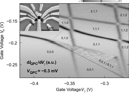
Figure 1. Charge stability diagram of a triple quantum dot measured with a QPC used as charge detector. Triples of integers denote electron numbers in the three QDs. A triangular region of telegraph noise is visible. Inset: micrograph of sample structure.
A similar situation can arise in a serial double quantum dot if one of the tunneling barriers between a quantum dot and the adjacent lead is closed. This QD can then only be charged via the other QD which again leads to slow and therefore observable tunneling processes. By varying the bias voltage of the QPC, the influence of the detector on the tunneling rates could be demonstrated (Fig. 2).
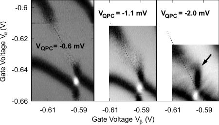
Figure 2. Part of a charge stability diagram of a double quantum dot with one tunnel barrier closed, measured with three different QPC bias voltages VQPC. A higher bias voltage causes changes in the tunneling rates, leading to a distortion of the charging lines.
- D. Taubert, M. Pioro-Ladrière, D. Schröer, D. Harbusch, A. S. Sachrajda, and S. Ludwig, Phys. Rev. Lett. 100, 176805 (2008)
- S. Gustavsson, R. Leturcq, B. Simovic, R. Schleser, T. Ihn, P. Studerus, K. Ensslin, D. C. Driscoll, and A. C. Gossard, Phys. Rev. Lett. 96, 076605 (2006)
Hyperfine Interaction in Laterally Defined Quantum Dots
Dawid Kupidura, Jörg P. Kotthaus, and Stefan Ludwig,
in collaboration with Werner Wegscheider
Spin-Qubits based on electrons defined in laterally defined quantum dots are promising candidates for quantum information processing schemes and subject of intensive research world-wide. While their principle suitability has been proven we are still in a stage of fundamental research on the level of one or two coupled qubits. Initialization and readout of single spins via spin-to-charge conversion has been successfully demonstrated in several labs. However, one of the still remaining problems is the limitation of the coherence time by the hyperfine interaction with nuclear-spins. There are two alternative paths to overcome this problem: The more intuitive one is to get rid of as many nuclear-spins as possible. This approach is realized within a collaboration with J. Sailer, D. Bougart and G. Abstreiter, all at the TU-München, using isotope clean and virtual nuclear-spin free SiGe-heterostructures [1]. In the second approach we rely on the high quality and well established GaAs/AlGaAs-heterostructures containing many nuclei with sizable magnetic moments. Here it is essential to reduce decoherence caused by the interaction with fluctuating nuclear spins being an unavoidable part of the system. We perform transport measurements on double quantum dot (QD) devices containing an integrated nanomagnet producing an inhomogeneous local magnetic field. Along this path we have studied the dynamics of the hyperfine interaction between nuclear spins and a single electron spin inside the double QD which is tuned into Pauli-spin blockade. Figure 1 displays a charge stability diagram of a double QD at finite bias. In this special configuration the inhomegenous magnetic field causes spin blockade in three out of four regions (triangles) of finite bias.
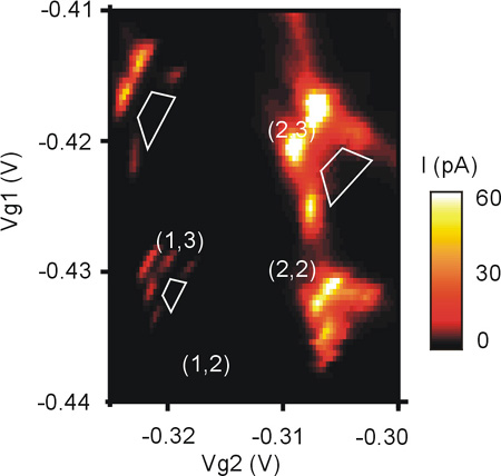
Figure 1. Current measured through a serial double QD device as a function of plunger gate voltages Vg1 and Vg2 for a Voltage VSD = 600uV applied across the device. Regions of spin blockade are framed by white tetragones. The number of electrons charging the two quantum dots in ground state configurations are depicted as pairs of numbers. Measurements are performed in a dilution refrigerator with a base temperature of 20 mK.
- J. Sailer, et al., Phys. Status Solidi RRL 3, No. 2, 61-63 (2009)
Freely suspended quantum dots
Clemens Rössler, Martin Herz, Jörg P. Kotthaus and Stefan Ludwig
in collaboration with Alexander W. Holleitner, Max Bichler, Dieter Schuh, and Werner Wegscheider
In this project an electro-optical hybrid system is realized employing a freely suspended quantum point contact (QPC). Our nanoscale bridges are excavated from AlGaAs/GaAs heterostructures containing a two-dimensional electron system (2DES). The 2DES is further structured by etched notches in order to define a one-dimensional-constriction (QPC). In-plane sidegates containing a 2DES are used to capacitively tune the device presented in Fig. 1.
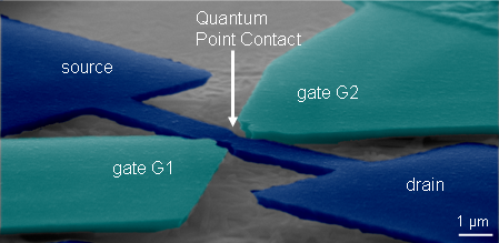
Figure 1. Scanning electron micrograph, taken under a tilt angle of 75 degrees, of a freely suspended bridge containing a narrow constriction and two inplane side gates. Colored regions inherit the 2DES.
Shining light onto this device we excite electron-hole pairs in addition to the intrinsic charge carriers of the 2DES. In the freely suspended device electron-hole pairs excited in the substrate cannot bypass the QPC being separate from the substrate. Nevertheless we observe a photo-response, i.e. a photo-induced increase of the conductance as shown in Fig.2.
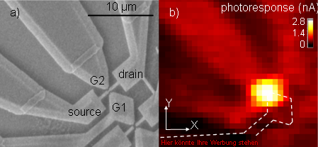
Figure 2. a) Scanning electron micrograph (top view) of the device also shown in Fig. 1. The active layer resides on a socket which is edgewise undercut (pale stripes). The submicron sized bars are fully suspended. b) Spatially resolved photoresponse. The scanned area is identical to the one in a), with the contour of the biased Gate G1 shown as dashed white lines as a guide to the eyes.
The origin of the observed photo-response can be explained in terms of an increase of charge carriers due to the excitation of electron-hole pairs (global effect). The strong conductance increase when shining light right onto the QPC (local effect) is understood in terms of a photo gating effect, where positive holes are collected at the edges of the suspended structure, thus acting as a positive gate voltage [1].
- C. Rossler, K.-D. Hof, S. Manus, S. Ludwig, J.P. Kotthaus, J. Simon, A.W. Holleitner, D. Schuh, W. Wegscheider, Appl. Phys. Lett. 93, 071107 (2008).
Optical and optoelectronical phenomena in nanodevices
The photoconductive response of quantum wires was explored by Klaus-Dieter Hof and Clemens Rössler et al. in experiments with high spatial and temporal resolution. Bernd Zebli et al. successfully created hybrid nanodevices consisting of CdTe nanocrystals bound to carbon nanotubes and studied the optical sensitization of the photoconductive response of the carbon nanotubes by the nanocrystals. All studies aim at creating increasingly complex artificial nanosystems with specifically tailored optical and optoelectronic responses. The optical excitation of carriers in man-made nanosystems resulting in both characteristic optical responses such as absorption, scattering and reemission of photons as well as in photon-induced modifications of the conductance continue to be a focus of our activities. Martin Kroner and collaborators have achieved a wealth of stimulating results in their studies of the optical response of carriers in individual self-assembled quantum dots embedded in voltage-tunable devices, employing high resolution luminescence and laser spectroscopies. Xaver Vögele et al. continued to explore the dynamics of dipolar excitons in double quantum wells confined by tailored electrostatic potentials to one dimensions.
Dynamic photoconductive gain effect in shallow-etched AlGaAs/GaAs quantum wires
Klaus-Dieter Hof, Clemens Rössler, J.P. Kotthaus, Alexander W. Holleitner in collaboration with A.W. Holleitner (TU München) and D. Schuh, W. Wegscheider (Universität Regensburg, Germany)
Klaus-Dieter Hof et al discovered a dynamic photoconductive gain effect in quantum wires which are lithographically fabricated in an AlGaAs/GaAs quantum well via a shallow-etch technique [1], [2]. The effect allows resolving the one-dimensional subbands of the quantum wires as maxima in the photoconductance across the quantum wires. The authors interpret their results by optically induced holes in the valence band of the quantum well which shift the chemical potential of the quantum wire. The non-linear current-voltage characteristics of the quantum wires allowed the authors detecting the photoconductive gain effect of excess charge carriers in the conduction band of the quantum well. The dynamics of the photoconductive gain are limited by the recombination time of both electrons and holes [1].

Figure 1A: Experimental circuit to detect the photoconductive gain effect in low-dimensional circuits: A lateral constriction of a 2DEG forms a quantum wire between source and drain contacts. The central area of the device is covered with an opaque gate bright rectangle. An aperture in this top gate close to the constriction defines the position where the underlying 2DEG of the source region is optically excited. B and C: The quantum wire is defined by two adjacent trenches A and B in the 2DEG via a shallow-etch technique [1]. D: Conductance and photoresponse data of sample A at Tbath = 2.3 K, fchop=117 Hz, and VSD=1.5 mV [2].
- Klaus-Dieter Hof, Clemens Rössler, Werner Wegscheider, Stefan Ludwig, Alexander Holleitner, Physica E 40, Issue 6, 1828 (2008).
- Klaus-Dieter Hof, Clemens Rössler, Stefan Manus, Jörg Kotthaus, Alexander Holleitner, Dieter Schuh, Werner Wegscheider, Phys. Rev. B 78, 115325 (2008)
Optoelectronic Sensitization of Carbon Nanotubes by CdTe Nanocrystals
B. Zebli, H.A. Vieyra, J.P. Kotthaus
in collaboration with A.W. Holleitner (TU München),
Achim Hartschuh (LMU München)
Itai Carmeli (Tel Aviv University, Israel)
B. Zebli et al. bound CdTe nanocrystals to single-walled carbon nanotubes via molecular recognition of the linker molecules biotin and streptavidin [Fig. 1(a)]. The authors investigated the photoconductance properties of such a carbon nanotube-nanocrystal-hybrids. B. Zebli et al. found that the photoconductance of the hybrids can be adjusted by the absorption characteristics of the nanocrystals. The photoconductance of the hybrid systems shows contributions of different relaxation optoelectronic processes. The observations are consistent both with a bolometrically induced current increase in the nanotubes caused by photon absorption in the nanocrystals and with a Förster resonance energy transfer from the nanocrystals to the nanotube [1].
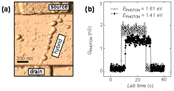
Fig. 1. (a) Atomic force microscope (AFM) image of an individual nanotube-nanocrystal-hybrid contacted by source and drain electrodes made out of Pd. The carbon nanotubes build the backbone of the hybrid structure, while the spherical particles in the AFM image are the CdTe nanocrystals. (b) Typical photoconductance measurement of an ensemble sample made of nanotube-nanocrystal-hybrids as a function of the laboratory time at EPHOTON = 1.61 eV (open circles) and EPHOTON = 1.41 eV (black circles). The authors find an enhanced photoconductance at photon energies larger than the recombination energy of the CdTe nanocrystals at ~1.59 eV [1].
- B. Zebli, H.A. Vieyra, I. Carmeli, A. Hartschuh, J.P. Kotthaus, A.W. Holleitner, arxiv 0807.2111.
Density Enhanced Diffusion of Dipolar Excitons within a One-Dimensional Channel
X. P. Vögele and J. P. Kotthaus,
in collaboration with A. W. Holleitner (TU München), D. Schuh, W. Wegscheider (Universität Regensburg)
Excitons with the electron and the hole separated in two different quantum wells are called dipolar excitons. A small tunnel barrier between the quantum wells causes a relatively long recombination lifetime of the dipolar excitons of up to several microseconds. This property and the fact that the excitons are bosons, makes it interesting to investigate their collective properties like superfluidity and Bose-Einstein-condensation at high exciton densities and low temperatures. To achieve a high dipolar exciton density it is necessary to trap them within the two-dimensional (2D) quantum well plane.
Recently, A. Gärtner reported on a new method to trap dipolar excitons within one-dimensional (1D) channels [1],[2]. We now investigated the lateral expansion of the excitons along such a 1D channel and compared the dynamics to the exciton expansion in the free 2D quantum well [see Figure]. In 2D we observe an exciton expansion that obeys non-linear temporal dynamics due to the repulsive dipole pressure at a high exciton density, in accordance with recent reports [3]. In contrast, the observed 1D expansion behaves linearly in time even at high exciton densities [4]. The corresponding 1D diffusion coefficient exceeds the one in 2D by far and depends linearly on the exciton density. We attributed the findings to screening of quantum well disorder by the dipolar excitons.
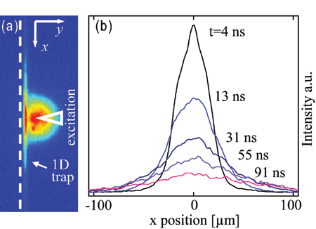
Figure 1: Spatial image of a typical photoluminescence (PL) distribution. Dashed line indicates the edge of the SiO2-layer that is on top the heterostructure. Close to the edge the excitons are trapped in a quasi 1D channel. (b) Line cuts of the exciton PL along the 1D channel at delay times t = 4 ns, 13 ns, 31 ns, 55 ns, 91 ns after the laser excitation.
- A. Gärtner, L. Prechtel, D. Schuh, A. W. Holleitner, and J. P. Kotthaus, Phys. Rev. B 76, 085304 (2007).
- A. Gärtner, D. Schuh, A. W. Holleitner, and J. P. Kotthaus, Physica E 40, 1828 (2008).
- Z. Vörös, et al., Phys. Rev. Lett. 94, 226401 (2005).
- X. P. Vögele, D. Schuh, W. Wegscheider, J. P. Kotthaus, and A. W. Holleitner, arXiv:0901.4875v1 (2009)
Nanomechanical systems
Nanomechanical systems are free-standing nanostructures with nanoscale cross-sections and lengths of several 10 to 100 microns. We investigate the resonant mechanical properties of a variety of such nanosystems ranging from high stress amorphous silicon nitride, over single crystal gallium arsenide to commercially available AFM cantilevers. While silicon nitride subject to high tensile stress allows to investigate high Q doubly clamped resonators, which can be employed to realize a nanomechanical charge shuttle, gallium arsenide can be etched to form large arrays of vertical pillars with interesting mode distribution. Another aspect of our research is cavity optomechanics, where the coupling of mechanical and optical degrees of freedom are investigated both experimentally and theoretically. An example of an optomechanical system is a Fabry-Perot cavity with a moveable mirror, as can be realized by an AFM cantilever. This seemingly simple system gives rise to backaction and extremely rich nonlinear dynamics. In order to increase the observed backaction, it would be favourable to employ nanostructured mechanical elements. To this end we theoretically study the optomechanical coupling of photonic crystal mirrors which exhibit a strong Doppler effect, or subwavelength-sized nanoresonators which experience scattering-induced backaction.
Ultrasonically driven nano-mechanical single-electron shuttle
Daniel R. König, Eva M. Weig, and Jörg P. Kotthaus
The transport and detection of single electrons with extraordinary precision has been a long sought goal since its potential impact on metrology was recognized in the 80s. For example, the one-by-one electron transfer with a well defined frequency may ultimately lead to the realisation of a quantum standard for the electrical current unit ampere – like the ones already implemented for voltage and resistance based on the Josephson and Quantum Hall effect, respectively. One possible approach to this goal is the mechanical transfer of single electrons. For this purpose a mechanical single electron shuttle was developed, which consists of a gold island situated in the center of a doubly clamped freely suspended nanoresonator (Fig. 1a).
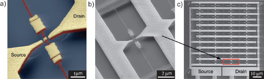
Figure 1. (a) A false-colour scanning electron microscope (SEM) micrograph of a single-electron-shuttle. A gold (yellow) island is located at the centre of a doubly clamped freely suspended silicon nitride (red) string. The gold island can shuttle electrons between the source and drain electrodes when excited by ultrasonic waves. (b) An SEM image taken at an angle showing a complete single-electron shuttle together with the clamping points of the freely suspended string. (c) An SEM image showing a top view of an array of 44 single-electron shuttles, which are connected in parallel between two interdigitated comb electrodes.
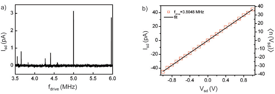
Figure 2. (a) Time-averaged source drain current Isd of an array with several nano-mechanical electron shuttles as function of the excitation frequency fdrive. Each of the eight resonances corresponds to a different shuttle of the array, which is mechanically excited at its eigenfrequency. (b) Source-drain current Isd as function of the source-drain voltage Vsd for one shuttle, which is excited at its eigenfrequency. The I-V-curve shows linear behaviour as expected by theory.
The samples are mechanically excited by ultrasonic waves and placed within a Faraday cage to shield it from undesired electromagnetic fields. In this configuration, electrically undisturbed mechanical electron transport at temperatures as low as 20 Kelvin was demonstrated (Fig. 2b). In this high temperature limit, excellent agreement between the measured data and theoretical calculations was observed [1].
- Koenig D. R., Weig E. M. and Kotthaus J. P., Nature Nanotechnology 3, 482 (2008).
Statistical analysis of arrays of pillar resonators
Philipp Paulitschke, Matthias Benecke, Heribert Lorenz, Eva M. Weig, Jörg P. Kotthaus
We fabricated arrays (14 x 14) of micron-sized pillars by electron beam lithography followed by reactive ion etching (Fig. 1a). In order to study the mechanical response of the array, pillars are globally mechanically excited via a piezo transducer. Under the optical microscope vibrating pillars appear blurred out, the image displaying the envelope of the mechanical mode. The high aspect ratio pillars show eigenfrequencies of the fist transverse harmonic mode between 0.1- 7 MHz and a quality factor around 1000 at atmospheric pressure. The broad distribution of pillar eigenfrequencies of about 50 kHz (Fig. 1b) can be fully attributed to geometrical deviations from the anticipated pillar shape.
This behaviour changes drastically when increasing the array size from 14x14 to 64x64 pillars. Instead of a smooth distribution of pillar frequencies, sharp resonances are observed at which a large number of pillars vibrate simultaneously. This behaviour might be attributed to an enhanced geometrical homogeneity of the pillar field, or to the coupling of the resonators. The investigation of the underlying mechanisms is the aim of ongoing investigations.


Figure 1. (a) Scanning electron micrograph of a 14 x 14 pillar array. The central 36 pillars indicated in red have been investigated for the statistical analysis of mechanical eigenfrequencies. (b) Histogram of the resonance frequencies determined for the first transverse eigenmodes of the central 36 pillars in the array shown in (a)
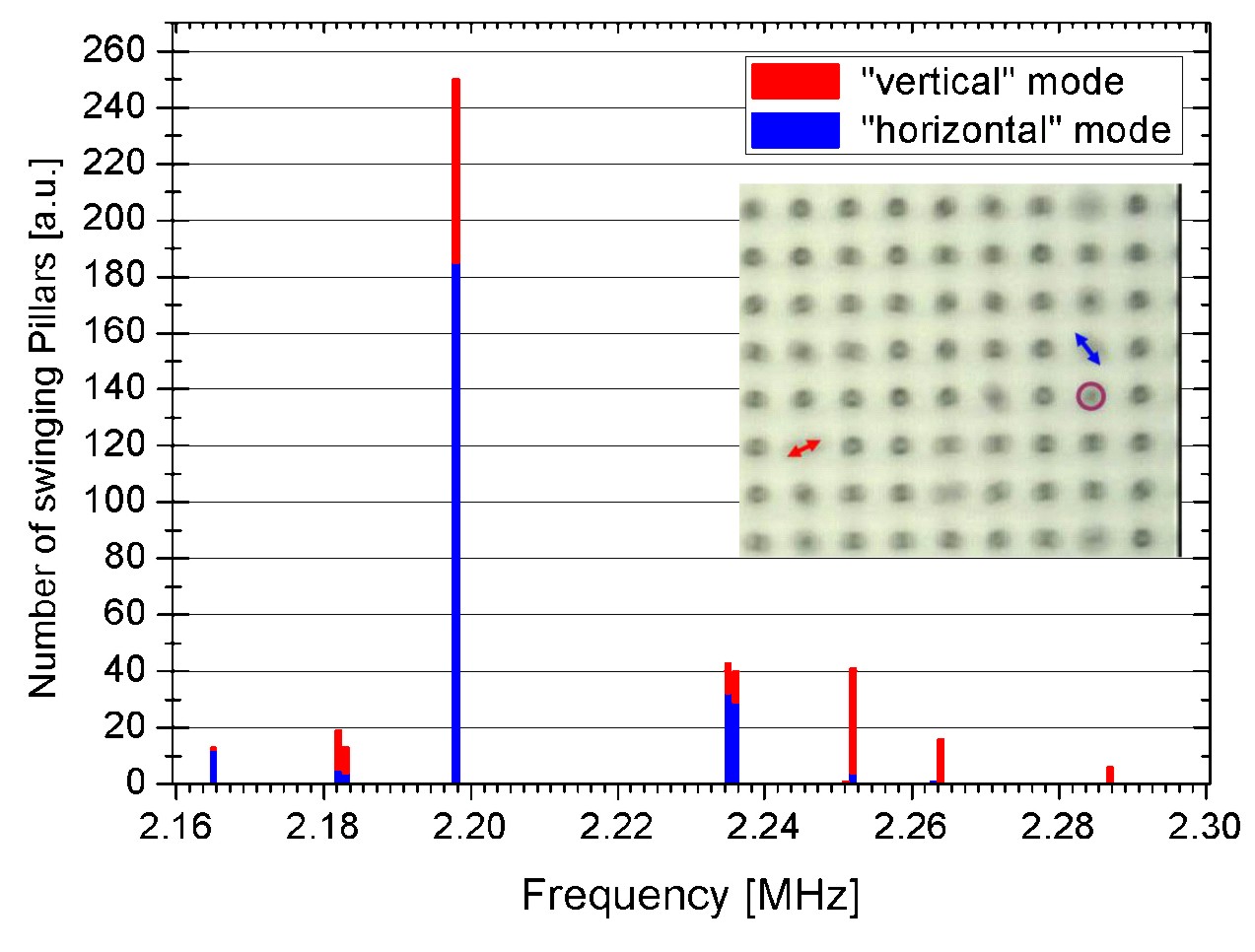
Figure 2. In the 64 x 64 array, the central 14 x 14 pillars have been investigated optically for the statistical analysis of the mechanical eigenfrequencies. The histogram shows the resonance frequencies determined for the first two orthogonal eigenmodes, indicated in red for the “vertical” and in blue for the “horizontal” mode of the central pillars of the array. The inset shows the center of the array and highlights examples of the observed modes.
Non-linear dynamics in opto-mechanical systems
Ivan Favero, Constanze Metzger, Alexander Ortlieb, Khaled Karrai In collaboration with Florian Marquardt, Max Ludwig, Clemens Neuenhahn
The intriguing idea of cooling a mechanical resonator with light has received considerable interest over the last years. Similar to laser cooling of single atoms, a part of the vibration energy of a cantilever can be transferred into photon energy and carried away by light [1]. In collaboration between F. Marquardt and K. Karrai, the inverse effect - exciting cantilever vibration by illumination - was explored [2]. In an experiment dominated by bolometric forces, strong nonlinear behavior of the cantilever motion was achieved. Although the basic instability has been observed by now in a number of experiments, it was recently realized theoretically that the nonlinear dynamics of this system can become highly nontrivial, leading to an intricate attractor diagram. We present an experiment that traces this diagram and offer a detailed analysis and comparison against theory. As an unexpected feature, we observe the simultaneous excitation of several mechanical modes of the cantilever, leading to coupled nonlinear dynamics. The comparison with theory has revealed the onset of multimode dynamics at large power, with two mechanical modes of the cantilever participating in the radiation-driven self-sustained oscillations. These effects could find applications in highly sensitive force or displacement detection.
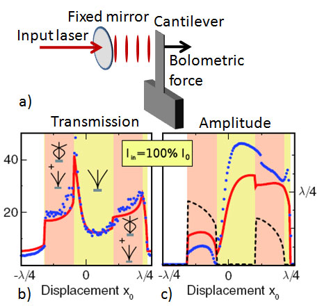
Figure 1 a) Coupling mechanical modes of a cantilever with optical modes of a cavity: a cantilever is subjected to light induced forces by a standing light wave trapped in a cavity. Fig b) and c) show the optical transmission of the cavity and the cantilever amplitude with cantilever displacement.
- Metzger C., Favero I., Ortlieb A., and Karrai K. Optical self cooling of a deformable Fabry-Perot cavity in the classical limit, Phys. Rev. B 78, 035309 (2008).
- Metzger C., Ludwig M., Neuenhahn C., Ortlieb A., Favero I., Karrai K., and Marquardt F. Self-Induced Oscillations in an Optomechanical System Driven by Bolometric Backaction, PRL 101, 133903 (2008).
Doppler Optomechanics of a Photonic Crystal
K. Karrai, I. Favero, and C. Metzger
A laser beam directed at a mirror attached onto a flexible mount adds friction to its mechanical motion by the Doppler effect. For a normal mirror the efficiency of this radiative Doppler friction is very weak and practically masked by laser shot noise. We find that it can become very efficient using a photonic crystal mirror near its photonic band gaps. As an example, a Bragg mirror used at the long wavelength edge of its band stop can be efficiently optically cooled using the Doppler friction. The opposite effect opens new routes for optical pumping of mechanical systems: a laser pointing at a Bragg mirror and tuned at its short wavelength edge induces amplification of the vibrational excitation of the mirror leading eventually to its self-oscillation. This could provide a very simple and noninvasive method to optically pump the motion of tiny mechanical resonators used in high sensitivity force detection. These new effects rely on the strong dependency of a photonic crystal reflectivity on the wavelength.
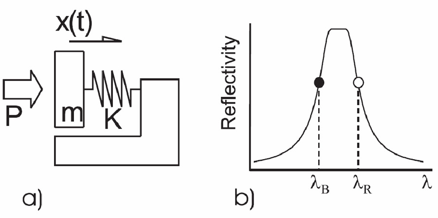
FIG. 1. (a) Doppler cooling of a photonic crystal: Schematics of a mirror of the wavelength dependent reflectivity R(l) and mass m mechanically attached and thermally anchored to a spring of rigidity K. The friction mechanisms internal to the spring are responsible for losses of mechanical energy. A laser of power P is directed at the mirror from the left. (b) Schematics of the reflectivity wavelength dependency of a Bragg mirror. The gradients of R are maximized at the edges of the mirror band stop.
- Karrai, K., Favero, I., and Metzger, C., Doppler Optomechanics of a Photonic Crystal, Phys. Rev. Lett, 100 240801 (2008).
Cavity cooling of a nanomechanical resonator by light scattering
I. Favero and K. Karrai
We present a novel method for opto-mechanical cooling of subwavelength-sized nanomechanical resonators [1]. Our scheme uses a high-finesse Fabry–Perot cavity of small mode volume, within which the nanoresonator acts as a position-dependent perturbation by scattering. In return, the back-action induced by the cavity affects the nanoresonator dynamics and can cool its fluctuations. We investigate such cavity cooling by scattering for a nanorod structure and predict that ground-state cooling is within reach. We have studied an optical cavity-cooling scheme of a nanomechanical resonator scattering photons within a high finesse Fabry–Perot cavity. This geometry, on top of allowing the use of subwavelength-sized objects, offers the possibility of engineering separately ultra-high-finesse cavities on the one hand and high-quality factor mechanical resonators on the other, an issue usually limiting opto-mechanical cooling experiments. Cavity-cooling in a purely dispersive limit and in a detuned cavity was discussed for atoms and molecules and very recently for a macroscopic membrane. Our scheme relies on a tuned cavity and in contrast to molecules or atoms, the nanoresonator is attached to a holder and cannot escape out of the cavity, offering the possibility of setting the motion of the nanoresonator into self-oscillation. The onset of nonlinear opto-mechanical behavior in this new situation of intense coupling between nanomechanics and optics will require a more complete theory, as developed in for studying multi-stabilities in Fabry–Perot cavities. Optical control of vibration properties of nanomechanical systems would open new routes, not only for sensing applications, but also for testing the quantum mechanical description of tiny objects.
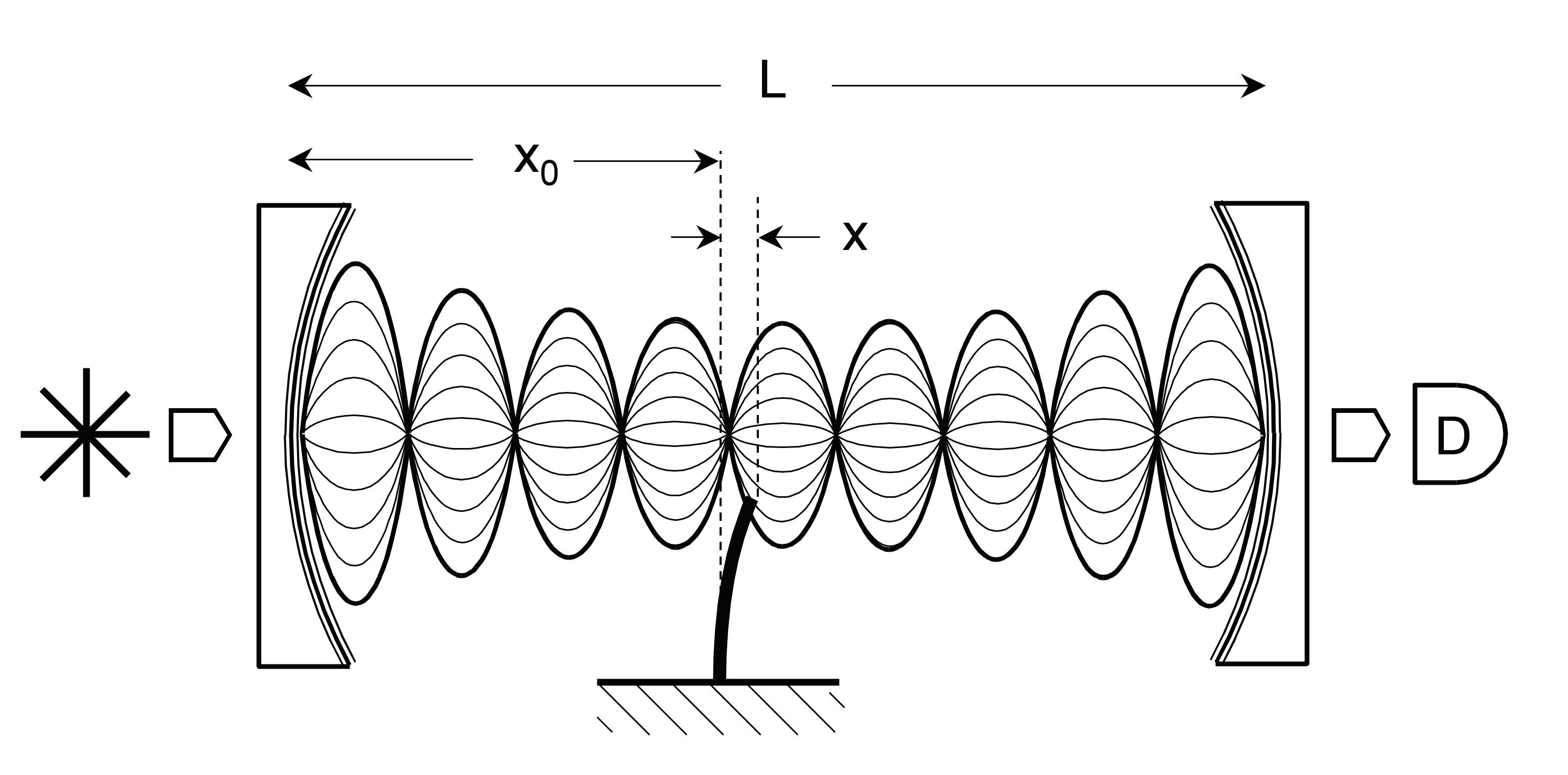
Figure 1: A nanomechanical resonator scattering photons in a high-finesse Fabry–Perot cavity, resonantly coupled to a laser on its left-hand side.
- Favero, I., and Karrai, Cavity cooling of a nanomechanical resonator bylight scattering, New J. Phys. 10, 095006 (2008).
Diploma theses completed in 2008
- Andreas Josef Fischer
"Funktionalisierte Nanopartikel als Drug-delivery-Systeme" - Jose Horas Aznar
"Investigation on unconventional aspects in the quantum Hall regime on narrow gate defined channels" - Christine Lux
"AC-Starkeffekt Messungen an einzelnen ladungsdurchstimmbaren Quantenpunkten" - Michael Müller
"Switching Phenomena in a Disordered System of Two Coupled Quantum Wires" - Daniela Taubert
"Wechselwirkungseffekte in parallelen und seriellen Doppelquantenpunktstrukturen" - Stefan Schwalb
"Charakterisierung des Resonanzverhaltens piezoelektrisch getriebener nanomechanischer Resonatoren aus zugverspanntem Siliziumnitrid" - Markus Stallhofer
"Untersuchung indirekter Exzitonen in gekoppelten InGaAs-Quantentöpfen"
PhD theses completed in 2008
- Martin Kroner
"Resonant photon-exciton interaction in semiconductor quantum dots" - Daniel König
"Nano-mechanischer Einzel-Elektronen-Transistor " - Clemens Rössler
"Elektronische und optische Eigenschaften freitragender Nanostrukturen" - Christian Dupraz
"Elektrooptische und elektromechanische Charakterisierung von Carbon Nanotubes"
Guest scientists in 2008
- Prof. Alexander Holleitner,
Technische Universität München, Walter Schottky Institut - Prof. Friedrich Simmel,
Technische Universität München - Prof. Khaled Karrai,
attocube systems, München - Prof. Richard Warburton,
Department of Physics, Heriot-Watt University, Edinburgh, UK, SFB 631 - Dr. Vadim Khrapay,
Russian Academy of Sciences, Chernogolovka, Russia, Alexander von Humboldt Stiftung - Prof. Alexander O. Govorov,
Ohio University, "Bessel award" der Alexander von Humboldt Stiftung - Dr. Ivan Favero,
Ecole Normale Supèrieure, Paris Cedex, France, Alexander von Humboldt Stiftung - Dr. Song Li,
Chinese Academy of Science, Beijng, China, Alexander von Humboldt Stiftung
Group members in 2008
Senior scientists
- Prof. Jörg P. Kotthaus
- Prof. Alexander Hoegele
- Dr. Heribert Lorenz
- Dr. Stefan Ludwig
- Dr. Eva-Maria Weig
Secretary
- Martina Jüttner
Technical staff
- Philipp Altpeter
- Hans-Peter Kiermaier
- Wolfgang Kurpas
- Stephan Manus
- Reinhold Rath
Ph.D. students
- Matthias Fiebig
- Daniel Harbusch
- Klaus-Dieter Hof
- Daniel König
- Martin Kroner
- Dawid Kupidura
- Michael Olapinski
- Philipp Paulitschke
- Clemens Rössler
- Georg Schinner
- Daniela Taubert
- Quirin Unterreithmeier
- Xaver Patrick Vögele
- Bernd Zebli
Diploma students
- Thomas Faust
- Christine Lux
- Johannes Mösl
- Michael Müller
- Leonhard Prechtel
- Johannes Rieger
- Florian Seilmeier
- Julian Schauseil
- Stefan Schwalb
- Sebastian Stapfner
- Markus Stallhofer
- Daniela Taubert
Publications in 2008
- M. Kroner, A. O. Govorov, S. Remi, B. Biedermann, S. Seidl, A. Badolato, P. M. Petroff, W. Zhang, R. Barbour, B. D. Gerardot, R. J. Warburton, and K. Karrai
"The nonlinear Fano effect"
Nature 451, 311-314 (2008). - F. W. Beil, A. Wixforth, W. Wegscheider, D. Schuh, M. Bichler, and R. H. Blick
“Shock Waves in Nanomechanical Resonators”
Phys. Rev. Lett. 100, 026801 -1--4 (2008). - B. D. Gerardot, D. Brunner, P. A. Dalgarno, P. Öhberg, S. Seidl, M. Kroner, K. Karrai, N. G. Stoltz, P. M. Petroff, and R. J. Warburton
"Optical pumping of a single hole spin in a quantum dot"
Nature 451, 441-444 (2008). - M. Kroner, C. Lux, S. Seidl, A. W. Holleitner, A. Badolato, P. M. Petroff, R. J. Warburton, and K. Karrai
"Rabi splitting and ac-Stark shift of a charged exciton"
Appl. Phys. Lett. 92, 031108 -1 - -3 (2008). - A. Hoegele, S. Seidl, M. Kroner, K. Karrai, C. Schulhauser, O. Sqalli, J. Scrimgeour, and R. J. Warburton
“Fiber-based confocal microscope for cryogenic spectroscopy”
Rev. Sci. Instrum. 79, 023709 -1 - -7 (2008). - B. Nickel, M. Fiebig, S. Schiefer, M. Goellner, M. Huth, C. Erlen, and P. Lugli
“Pentacene devices: Molecular structure, charge transport and photo response”
phys. stat. sol. (a) 205, 526–533 (2008). - K.-D. Hof, C. Rossler, W. Wegscheider, S. Ludwig, A. W. Holleitner
"Optically induced charge transport through submicron channels"
Physica E 40 1739–1741 (2008). - M. Olapinski, S. Manus, N. Fertig, F. C. Simmel
“Probing whole cell currents in high-frequency fields: Identification of thermal effects”
Biosens. Bioelectron. 23, 872-878 (2008). - C. Rossler, M. Bichler, D. Schuh, W. Wegscheider and S. Ludwig
“Laterally defined freely suspended quantum dots in GaAs/AlGaAs heterostructures”
Nanotechnology 19, 165201 (2008). - V. S. Khrapai, S. Ludwig, J. P. Kotthaus, H. P. Tranitz, W. Wegscheider
"Nonequilibrium phenomena in adjacent electrically isolated nanostructures"
Physica E 40, 995-998 (2008). - J. Horas, A. Siddiki, J. Moser, W. Wegscheider and S. Ludwig
"Investigations on unconventional aspects in the quantum Hall regime of narrow gate defined channels"
Physica E 40, 1130-1132 (2008). - A. Gärtner, D. Schuh, A. W. Holleitner, and J. P. Kotthaus
"Loading indirect excitons into an electrostatic trap formed in coupled GaAs quantum wells"
Physica E 40, 1828–1831 (2008). - S. Seidl, M. Kroner, C. Lux, A. W. Holleitner, K. Karrai, R. J. Warburton, A. Badolato, and P. M. Petroff
"Resonant transmission spectroscopy on the p to p transitions of a charge tunable InGaAs quantum dot"
Appl. Phys. Lett. 92, 153103 -1 - -3 (2008). - M. Kroner, K. M. Weiss, B. Biedermann, S. Seidl, S. Manus, A. W. Holleitner, A. Badolato, P. M. Petroff, B. D. Gerardot, R. J. Warburton, and K. Karrai
“Optical Detection of Single-Electron Spin Resonance in a Quantum Dot”
Phys. Rev. Lett. 100, 156803 -1 - -4 (2008). - M. Kroner, S. Remi A. Hoegele, S. Seidl, A. W. Holleitner, R. J. Warburton, B. D. Gerardot, P. M. Petroff, and K. Karrai
"Resonant saturation laser spectroscopy of a single self-assembled quantum dot"
Physica E 40, 1994 - 1996 (2008). - S. Seidl, B. D. Gerardot, P. A. Dalgarno, K. Kowalik, A. W. Holleitner, P. M. Petroff, K. Karrai, R. J. Warburton
"Statistics of quantum dot exciton fine structure splittings and their polarization orientations"
Physica E 40, 2153-2155 (2008). - P A. Dalgarno, M. Ediger, B. D. Gerardot, J. M. Smith, S. Seidl, M. Kroner, K. Karrai, P. M. Petroff, A. O. Govorov, and R. J. Warburton
“Optically Induced Hybridization of a Quantum Dot State with a Filled Continuum” Phys. Rev. Lett. 100, 176801 -1 - -4 (2008). - D. Taubert, M. Pioro-Ladrière, D. Schröer, D. Harbusch, A. S. Sachrajda, and S. Ludwig
"Telegraph Noise in Coupled Quantum Dot Circuits Induced by a Quantum Point Contact"
Phys. Rev. Lett. 100, 176805 -1 - -4 (2008). - K. Karrai, I. Favero, and C. Metzger
"Doppler Optomechanics of a Photonic Crystal"
Phys. Rev. Lett. 100, 240801 -1 - -4 (2008) . - L. Song, A. W. Holleitner, H. Qian, A. Hartschuh, M. Doeblinger, E. M. Weig, and J. P. Kotthaus
"A Carbon Nanofilament-Bead Necklace"
J. Phys. Chem. C 112, 9644–9649 (2008). - L. Song, W. Ma, Y. Ren, W. Zhou, S. Xie, P. Tan, and L. Sun
"Temperature dependence of Raman spectra in single-walled carbon nanotube rings"
Appl. Phys. Lett. 92, 121905 -1 - -3 (2008). - D. R. Koenig, E. M. Weig, and J. P. Kotthaus
"Ultrasonically driven nano-mechanical single-electron shuttle"
Nat. Nanotechnol. 3 , 482-485 (2008). - C. Metzger, I. Favero, A. Ortlieb, and K. Karrai
"Optical self cooling of a deformable Fabry-Perot cavity in the classical limit"
Phys. Rev. B 78, 035309 -1 - -12 (2008). - M. Kroner, K. M. Weiss, B. Biedermann, S. Seidl, A. W. Holleitner, A. Badolato, P. M. Petroff, P. Öhberg, R. J. Warburton, and K. Karrai
"Resonant two-color high-resolution spectroscopy of a negatively charged exciton in a self-assembled quantum dot"
Phys. Rev. B 78, 075429 -1 - -13 (2008). - C. Rossler, K.-D. Hof, S. Manus, S. Ludwig, J. P. Kotthaus, J. Simon, A. W. Holleitner, D. Schuh, W. Wegscheider
"Optically induced transport properties of freely suspended semiconductor submicron channels"
Appl. Phys. Lett. 93, 071107 (2008). - K.-D. Hof, C. Rossler, S. Manus, J. P. Kotthaus, A. W. Holleitner, D. Schuh, W. Wegscheider
"Photoconductive gain effect in shallow-etched AlGaAs/GaAs quantum wires" Phys. Rev. B 78, 115325 -1 - -5 (2008). - C. Metzger, M. Ludwig, C. Neuenhahn, A. Ortlieb, I. Favero, K. Karrai, and F. Marquardt
"Self-Induced Oscillations in an Optomechanical System Driven by Bolometric Backaction "
Phys. Rev. Lett. 101, 133903 (2008). - V. S. Khrapai, S. Ludwig, J. P. Kotthaus, H. P. Tranitz, and W. Wegscheider
"Nonequilibrium interactions between two quantum circuits"
J. Phys.: Condens. Matter 20, 454205 (2008). - I. Favero and K Karrai
"Cavity cooling of a nanomechanical resonator by light scattering" New J. Phys. 10, 95006 (2008). - P. A. Dalgarno, J. McFarlane, D. Brunner, R. W. Lambert, B. D. Gerardot, R. J. Warburton, K. Karrai, A. Badolato, and P. M. Petroff
"Hole recapture limited single photon generation from a single n-type charge-tunable quantum dot"
Appl. Phys. Lett. 92, 193103 (2008) - P. A. Dalgarno, J. M. Smith, J. McFarlane, B. D. Gerardot, K. Karrai, A. Badolato, P. M. Petroff, and R. J. Warburton
" Coulomb interactions in single charged self-assembled quantum dots: Radiative lifetime and recombination energy"
Phys. Rev. B 77, 245311 (2008)
Invited talks in 2008
Jörg P. Kotthaus
- "Dynamics of quantum well excitons in tunable landscapes" Symposium on Magnetic Excitations in Semiconductors – Bridges to the next Decade University of Buffalo, USA March 07 - 08, 2008
- „Non-equilibrium quantum transport through GaAs-based nanostructures“ Bilateral Workshop on Nanoscale Systems, Nanasystems Initiative Munich and Global COE: Secure-Life Electronics, The University of Tokyo Ludwig-Maximilians-Universität München, Garching July 10, 2008
- „Non-equilibrium quantum transport through GaAs-based nanostructures“ Conference „Quantum Dynamics in Dots and Junctions: Coherent Solid State Systems“ Riva del Garda, Italy October 5-10, 2008
Eva Weig
- "Charge transport and nonlinear response of a nanomechanical shuttle" NIM Focus Workshop "Nonequilibrium thermodynamics at the nanoscale", September 24, 2008
Stefan Ludwig
- "Electronic Interaction in Coupled Quantum Systems" Joint Conferences on Interaction Among Nanostructures (VC-IAN) February 03 - 07, 2008, Orlando, Florida, USA
- "From Equilibrium - to Non-Equilibrium Interaction in Coupled Quantum Dot Devices" JST-DFG Workshop on Nanoelectronics March 05 -07, 2008, Aachen, Germany
- "Phonon-Mediated Non-Equilibrium Interaction between Mesoscopic Devices" Quantum Dynamics in Dots and Junctions: Coherent Solid State Systems Oct. 05-10, 2008, Riva del Garda, Italy
Senior scientists of cooperating groups
- Gerhard Abstreiter, Max Bichler, Dieter Schuh Walter Schottky Institut, TU München, Germany.
- S. James Allen University of California, Santa Barbara, USA.
- David Awschalom University of California, Santa Barbara, USA.
- Thomas Bein CeNS, LMU Munich, Germany.
- Robert Blick University of Wisconsin-Madison, USA.
- Alik Chaplik Institute of Semiconductor Physics, Novosibirsk, Russia.
- Valeri Dolgopolov Russian Academy of Sciences, Chernogolovka, Russia.
- Karl Eberl Max-Planck-Institut für Festkörperforschung, Stuttgart, Germany.
- Jochen Feldmann CeNS, LMU München, Germany.
- Niels Fertig Nanion GmbH, München, Germany.
- Jorge M. Garcia Instituto de Microelectronica de Madrid, Spain.
- Hermann Gaub CeNS, LMU Munich, Germany.
- Arthur C. Gossard Materials Department, University of California - Santa Barbara, USA.
- Alexander O. Govorov Ohio University, USA
- Theodor W. Hänsch LMU Munich, Germany.
- Wolfgang Heckl CeNS, LMU Munich, Germany.
- Atac Imamoglu Department of Physics, ETH Swiss Federal Institute of Technology, Zurich
- Karl-Heinz Kunzelmann Dental Science, LMU, Munich
- Don Lamb CeNS, LMU Munich, Germany.
- Paul Leiderer University of Konstanz, Germany.
- Axel Lorke Universität Duisburg-Essen, Germany.
- Wolfgang Parak CeNS, LMU Munich, Germany.
- Pierre M. Petroff University of California - Santa Barbara, USA.
- Joachim Rädler, Bert Nickel LMU München, Germany.
- Mansour Shayegan Princeton University, USA.
- Ulrich Schubert Eindhoven University of Technology, Dutch Polymer Institute, Eindhoven, Netherlands.
- Jan von Delft CeNS, LMU Munich, Germany.
- Richard Warburton Heriot-Watt University, Edinburgh, U.K.
- Werner Wegscheider, Christoph Strunk Institut für Angewandte und Experimentelle Physik, Universität Regensburg, Germany.
- Andreas Wieck Ruhr-Universität Bochum, Germany.
- Achim Wixforth Universität Augsburg, Germany.
Financial support in 2008
Funding of this work via the following agencies is gratefully acknowledged: