

Research report 1996
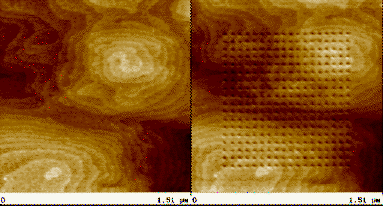
Figure 1. Atomic force microscopic image of an InAs surface quantum well structure before (left) and after (right) definition of a short scale antidot lattice. The artificial superlattice has been created by directly 'punching holes' into the active surface layer thus creating an array of repulsive potentials. The spiral-like fine structure represents atomic layer features on the as grown InAs surface.
Overview
Most of the modern electronic devices as used in state-of-the-art complex circuits like microprocessors etc. are nowadays based on so-called quasi-two-dimensional electtron systems (Q2DES). Such Q2DES can be realized at the interface between a semiconductor and an insulator, or at the interface between two semiconductors.
In a Q2DES, the electrons are confined along one spatial direction to within a length scale comparable to their quantum-mechanical wavelength. In the plane perpendicular to the direction of the confinement, however, they are more or less free to move.
Apart from a much better defined switching behavior and less power consumption as compared to many bulk-based semiconductor devices, the interface- and Q2DES- based devices also offer insight into many new and fascinating physical properties which are related to the reduced dimensionality.
Modern semiconductor physics concentrates on a further reduction of the dimensionality of the electron systems under investigation. Nowadays, so-called quantum wires (or quasi-one-dimensional electron systems Q1DES) and even quantum dots (Q0DES) can be realized. Here, the motion of an electron as confined in the repective artificial potential well is additionally quantized into a series of eigenstates. For quantum dots, this complete quantization is very similar to the one of the electron in an atom - this is why quantum dots are sometimes referred to as 'artificial atoms'. However, unlike to their real counterparts, the number of electrons per artificial atom may be tuned externally by, e.g. an electric field. Thus - we expect something like a revival of atomic physics if we continue to follow this tremendously interesting path.
In our research group here at the LMU, we study the properties of such electron systems which are confined to very small dimensions to form Q2DES, Q1DES and Q0DES as well as interactions between those low-dimensional systems. Also, the fundamental technologies to produce such systems are investigated and exploited. We concentrate on semiconductor structures based on the Si/SiO2 as well as compound semiconductor combinations such as GaAs/AlGaAs, InAs/AlSb, InAs/GaAs and related heterojunctions. Our work is based on several close collaborations with groups around the world that grow and characterize the above listed heterostructures with highest quality. Using different sophisticated facilities in our cleanroom lab we are able to laterally pattern the semiconductor structures down to lengthscales of only a few nanometers. We apply different lithografic techniques, such as holography, electron beam writing, and atomic force microscopy, which allow for a very flexible realization of very small sample sizes.
Experimentally, our setups provide the more or less unique opportunity to investigate our samples over a very wide frequency range from DC up to the UV region. We have access to several different high frequency setups (DC..20 GHz), a microwave vector network analyzer (8.5GHz..350 GHz), an (far-)infrared molecular laser, two (far-)infrared Fourier Transform Spectrometers and different laser systems, some of which are tuneable from the near infrared into the visible spectral range. All of our experimental setups are equipped with low-temperature cryostats and superconducting magnet systems, providing magnetic fields up to 15 Tesla. The combination of all our equipment and experimental facilities provides us with the basis for a detailed investigation of the new physical properties of semiconductor nanostructures.
A. Transport Properties
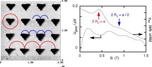
Figure 2. Microscopic image of a 'triangular' antiot lattice (left) and corresponding
magnetotransport- and photovoltage measurement in a magnetic field. The sketched
trajectories correspond to the pronounced features in the transport properties.
(The high quality heterostructure starting material for this project as well as
for many others reported here has been grown by W.
Wegscheider in the Walter-Schottky-Institute
in Garching.)
A.1. Interaction of Surface Acoustic Waves (SAW) and Low-Dimensional Electron Systems
Surface acoustic waves are modes of elastic energy which can propagate on the surface of different materials. If the substrate is piezoelectric, those waves are accompanied by electric fields which then propagate at the speed of sound. The electric fields of the wave can couple to the mobile carriers within a semiconductor structure and modify its electronic and elastic properties. By measuring the attenuation of the wave and the renormalization of the sound velocity we can, for instance, extract information on the dynamic conductivity of the electron system. We also investigate the possibility to use a SAW for a dynamical lateral potential modulation and we investigate the influence of a SAW onto the optical properties of an electron system. Our experiments presently cover the frequency range between 100 MHz and 6 GHz, corresponding to surface acoustic wavelengths between 30um and 0.5um, respectively.
In 1996 we focused on mainly two different topics, namely the realization of SAW-based hybrid structures consisting of a strong piezoelectric (LiNbO3) and a thin semiconductor layer structure that has been lifted off its natural substrate. Here, the SAW - 2DES interaction can be enlarged by two orders of magnitude as compared to the monolithic case. This interaction is now strong enough to become technologically very attractive. Together with the Siemens research lab, we are presently developping new concepts for a technological exploitation of this approach.
The second topic is the investigation of the acousto-optic interaction between a strong SAW and a semiconductor quantum well system. Here, a completely new and exciting area of research has been opened. We observe a strong influence of the SAW on the optical properties of a quantum well . The photoluminescence of the quantum well can be completely quenched under the influence of the SAW. Moreover, we show that the SAW can act as a "Photon Conveyor Belt", where optical signals can be stored by the SAW in the semiconductor and may be re-assembled into light after very long delay times and at a remote location of the sample!
Further, and related studies, namely the influence of SAW on the optical properties of semiconductor quantum structures aim towards the use of SAW for the generation of lateral Bragg gratings by a modulation of the local refractive index of the system. Such lateral, tunable grating structures will be of severe importance for future acousto-opto-electric devices like modulators, switches and multiplexers. This work is performed under the sponsorship of the Bayerische Forschungsverbund FOROPTO
A.2. Capacitance Spectroscopy on Single Field-Effect-Induced Electron Wires in AlGaAs-GaAs Heterostructures
In specially designed heterostructure crystals grown by M. Holland in Glasgow we use e-beam defined gate electrodes to generate 150mm long quantum wires with different widths. We perform capacitance spectroscopy to investigate the electronic properties of very high quality electron wires. Because of the very small capacitance involved we developed a capacitance bridge with an impedance transformer close to the sample. We show that the capacitance spectroscopy allows us to study the formation of compressible and incompressible strips in a 2D interacting electron plasma at high magnetic fields. In the case of broad electron channels (width ~300nm) at high magnetic fields we find that the capacitance minimum at the filling factor 2 is strongly asymmetric that is in an agreement with a model proposed by A. O. Govorov.
A.3. Electron Transport in Antidot-Lattices
"Antidot" lattices can be considered the complementary structure to quantum dot lattices: While in the latter, an array of isolated islands of electrons are created, in the former an array of small voids is cut out of a two-dimensional electron gas. In the past, a number of novel effects have been observed both in classical as well as quantum transport, which result from the interplay between different length scales in antidot-lattices (lattice period, magnetic length, Fermi-wavelength). Whereas commonly circular voids are patterned, we have created square lattices of triangular antidots, thus breaking the left-right symmetry of the electron system . In low frequency transport these samples exhibit maxima in the magnetotransport at a magnetic field where the cyclotron diameter equals half the lattice period. This is caused by so-called skipping orbits and shows that it is indeed possible to transfer triangular shapes with straight edges into the two-dimensional electron gas. In high-frequency experiments we observe lateral photo-voltages which closely reflect the features in low-frequency transport caused by the presence of the antidots. This might be due to the fact that the broken symmetry of the antidot-lattice leads to a rectification of the high-frequency radiation. Apart from triangular antidots a second research subject are short period antidot devices which are fabricated by atomic force microscope (AFM) lithography into shallow HEMTs. Here lattices with a"diatomic" basis consisting of two circular antidots were investigated. For a constant period we systematically varied the spacing between the antidots forming the basis. Magnetoransport investigations of these devices allow to distinguish between so called pinned orbits and run away trajectories and such give information on the the transport mechanism through such devices.
A.4. Coulomb Blockade Phenomena in Quantum Dots
The fluctuations and the distribution of the conductance peak spacings of a quantum dot in the Coulomb-blockade regime are studied and compared with the predictions of random matrix theory (RMT). The experimental data were obtained in transport measurements performed on a semiconductor quantum dot fabricated in a GaAs-AlGaAs heterostructure. Coulomb interactions of the electrons in a quantum dot can be described by a capacitive charging term. In this picture the gate voltage differences between adjacent conductance peaks should be given by the sum of a classical charging energy and the spacing between adjacent bare energy levels of the dot. Thus, after subtraction of the charging term, one should have direct access to the quantum dotps ener-gy level spectrum. As RMT provides a very good description of the statistical properties of the spectra of many complex systems, the level spacings obtained from Coulomb blockade measurements are also expected to obey its predictions. However, it is found that the fluctu-ations in the peak spacings are considerably larger than predicted by RMT. Furthermore, the distribution of the spacings does not obey the Wigner surmise, which follows from RMT, but rather appears Gaussian distributed around a mean value. This indicates that the fluctuations in the electronic interactions have an important influence on the statistics of the peak spacings. The peak spacings cannot be related to a noninteracting single particle spectrum, as suggested by the capacitive charging model, but display the ground state energy spacings of an interacting system. However, RMT was originally developed to handle the statistical properties of excitation spectra. So far, it is not clear whether the results of RMT can be applied to ground state energy statistics.
A.5. High Frequency Properties of Quantum Point Contacts and Quantum Dots
The non-linear transport properties of ballistic quantum point contacts are investigated and well understood nowadays. We employ these non linearities in the IV characteristic of ballistic point contacts to aim towards a high frequency signal processing. First experiments using ballistic point contacts as high frequency mixers are very promising in these terms. We develop techniques to efficiently couple high frequency radiation into the ballistic point contact by using lenses, antennae and multi point contact arays.
A.6. Electronic Phases in Two-Dimensional Systems
In close cooperation with the Institute of Solid State Physics in Chernogolovka, Russia (Prof. V.T. Dolgopolov and co-workers) we measure the magnetocapacitance at temperatures down to 25 mK on special high-mobility AlGaAs/GaAs heterostructures that have, apart from a top gate, a back electrode below the two-dimensional electron gas. Vertical transport establishes equilibrium between the electron gas and the back electrode so that even integer filling factors with vanishing dissipative conductivity are accessible to magnetocapacitance measurements. From our experimental data we extract the dependences of the thermodynamic density of states and of the quantum level width on both the position of the Fermi level and magnetic field. In the integer quantum Hall state at filling factor 2 the thermodynamic density of states remains finite in magnetic fields up to 8 T and is approximately a parabolic function. Its value is varied in a wide range (approximately by 2 orders of magnitude). The level width shows power-law energy and magnetic field dependences with an exponent of about 0.8. At even and odd filling factors the behaviour of the thermodynamic density of states proves to be similar. We find excellent agreement between our experimental results and the theory based on nonlinear screening. A collaboration with the theoretical group of A. V. Chaplik at the Institute of Semiconductor Physics in Novosibirsk (Russia) relates to electronic instabilities in quantum-dot arrays. To find experimental conditions for the appearance of ferro- (antiferro-) electric phase transitions, theorists from Novosibirsk discussed a molecular-like lateral array of quantum dots, where an elementary cell consists of two quantum dots connected by tunnelling. It was demonstrated theoretically that the type of a phase transition depends on symmetry of an array and the phase transition can be induced by application of a magnetic field (see A. V. Chaplik and A. O. Govorov, J. Phys.C8,4071 (1996))
A.7. Giant Growth of Quantum Oscillations in an Inhomogeneous 2D Electron System
In this research project done in close cooperation with the Institute of Solid State Physics in Chernogolovka, Russia (Prof. V.T. Dolgopolov and co-workers) and the Institute of Applied Physics in Hamburg (Prof. W. Hansen and co-workers) we experimentally find that the connection of 2D electron systems with different electrochemical potentials results in long-range ( 50 micrometer) electron density disturbances. When a gated region of the Corbino sample is strongly depleted, the amplitude of the magneto-resistance oscillations caused by high-density ungated regions is found to increase in proportion to the sample resistance which is dominated by low density regions with small conductivity. Experiments on samples with artificial potential profiles (antidots and etched rings) below the gate establish that contact effects are not the cause of the observed phenomena.
B. Intra- and Interband Spectroscopy
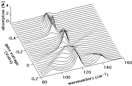
Figure 3. Intersubband-like absorptions of a strongly coupled double quantum well. In (a) we depict the possible transitions as calculated self-consistently. In (b) the corresponding experimental resonance positions are shown. The resonance positions agree very well with the theoretical prediction if a constant energetic offset simulating the effect of the depolarization shift is added to the single-particle trasition energies.
B.1. Electron Systems in Band Gap Engineered Quantum Systems
Modern crystal growth techniques like molecular beam epitaxy nowadays offer the unique advantage of tailoring the band edges of different semiconductor systems in a very controlled manner. A prominent example is the so-called parabolic quantum well (PQW), but also more complex systems can be realized.
In close co-operation with the research group of A.C. Gossard in Santa Barbara we concentrate on the investigation of the collective reponse of low-dimensional electron systems in such man-made semiconductor structures. As an example, the electron system in the parabolic quantum well represents in good approximation the concept of a free electron system in a homogenous positive background ('JELLIUM').
Recently, we also focused on the investigations of the properties in coupled quantum well structures on the basis of PQW. Here, too, the very precise control of the potential profiles in growth direction can be used to fabricate nearly any desired structure. For instance, in analogy to the term 'artificial atom' we study the properties of artificial 'molecules' using two coupled PQW as a simple but powerful model system.
Absorption experiments in the far infra-red have been carried out on superlattice samples based o the PQW approach. The electrons are excited within the first miniband or from the first to the second miniband. We see strong evidence that the inter-miniband transition changes from being collective to single-particle-like depending on the strength of the inter-well coupling. We have shown how a magnetic field applied perpendicular to the superlattice direction can be used to reduce the coupling between the wells. This can lead to the situation where the resonance is single-particle-like at zero magnetic field but collective at high magnetic field.
B.2.Intersubband Spectroscopy of InAs/AlSb Quantum Wells
The relatively small energy gap of some semiconductors like InAs and the related pronounced coupling of neighbouring bands leads to strong non-parabolic effects in the energy vs. momentum dispersion relation. Such a non-parabolicity reflects, e.g., in a strongly energy dependent effective mass. To study such effects we concentrate on a relatively new material combination, namely InAs/AlSb which also provides the deepest quantum wells available to date.
A number of experiments have demonstrated that the depolarisation field plays a very important role in the intersubband resonance of InAs quantum wells. In particular, we have shown that the width of the intersubband resonance is not influenced by the broad single-particle spectrum which arises from strong nonparabolicity in the energy dispersion. This leaves the question open as to which scattering mechanism determines the linewidth. In order to investigate this point we have measured the intersubband resonance linewidth against well width and against temperature. The results demonstrate that fluctuations in the well width dominate, even at temperatures well above room temperature. Theoretical work is underway to try and understand this behaviour in terms of a decay of the collective mode into single-particle transitions (Landau damping). We have also investigated the case in which the first and second subbands are occupied and we see very strong coupling effects between the two resonances. In particular, the 1-2 resonance becomes very broad at elevated temperature. This supports the Landau damping picture as the 1-2 collective mode can decay into energetically degenerate 2-3 single-particle transitions.
As many of our intersubband resonance absorption experiments are performed using a grating coupler technique, we investigated both experimenatlly as well as theoretically the influence of the grating design on the absorption of intersubband resonances in quantum well systems. It turns out that the design of the grating coupler strongly influences the lineshape and absorption strength of the observed resonances.
B.3. Photoconductive Response of Ins/AlSb Quantum Wells
Not only from the physics point of view this material combination is a very attractive candidate for semiconductor research. The unique band structure together with high carrier concentrations and small effective masses makes it very interesting for possible device applications. Here, we focus on the photonic properties and the optoelectronic response. Possible applications include infrared detectors, modulators, and switches in the infrared regime. In close co- operation with the research group of H. Kroemer at UC Santa Barbara (USA) we design and develop suitable layer structures to follow this route.
B.4. Influence of Infrared Excitation on the Low-Frequency Transport in Low-Dimensional Systems
The combination of DC transport and (far)-infrared excitation experiments offers a number of interesting opportunities. In these experiments, e.g., the sample itself serves as a detector, which is not only interesting from a technological point of view but also offers the advantage of local detection, which is of great benefit especially for samples which are smaller than the wavelength of the excitation radiation. Using this technique, we have investigated the dynamics of edge states in the quantum Hall effect. Because of very low scattering, these edge channels are in a way ideal one-dimensional model systems. However, spectroscopy on these channels proves to be extremely difficult because of the fact that they are strips of only ~ 0.5 um next to a much larger area of two-dimensional electron gas which absorbs in the same frequency regime. Using the edge channels as detectors, together with employing a micro-shadow mask technique, we were able to detect different excitations of quantum Hall edge states and obtain information on the local curvature of the edge potential in etched and gated Hall bars.
B.5. Spectroscopy of Self-Organized InAs Quantum Dots
With decreasing sizes of nanostructures the problem of homogeneity becomes more and more important. Ideally, one would like to study large arrays of identical quantum systems. One elegant way to achieve this is to use fabrication mechnisms where the shape and the dimensions of the nanostructures are given by, energetic considerations, such that energy minimization will lead to the desired sample homogeneity. This happens, e.g. in the Stranski-Krastanow growth mode of InAs on GaAs heteroepitaxy and results in layers of uniform quantum dots of ~ 20 nm diameter and ~ 7 nm height. In a close collaboration with the group of P. Petroff at UC Santa Barbara we have demonstrated that these dots can be integrated into a metal-insulator-semiconductor heterostructure, which allows us to tune the electron number per dot, determine it by capacitance spectroscopy, and study the dots' excitation in the far-infrared. Here, the far-infrared spectroscopy resembles the atomic spectroscopy mentioned in the introduction. Indeed, we can "tune the dots through the table of elements" and distinguish, e.g. "quantum dot Helium" and "quantum dot Lithium" by their excitation spectrum. Furthermore, we can directly compare the different ground states of these few-electron systems, and, from a comparison between ground state and excitation energies, derive detailed information on the Coulomb and quantization contributions to the energetic structure of these man-made "atoms". On small dot ensembles we observe a pronounced fine structure in the capacitance spectra which reflect ensemble properties and can be explained either by dot-dot-interctions or by monolayer fluctuations.
B.6.Optics on Field-Effect Induced Tuneable Potential Superlattices in AlGaAs-GaAs Heterostructures.
Voltage - controlled lateral superlattices are employed to demonstrate the trapping of photogenerated excitons in quasi- one dimensional regions and to store light in form of ionised excitons in the quantum well of a semiconductor heterostructure. Two interdigitated gate electrodes on the surface of a semiconductor heterostructure and a back electrode buried below the GaAs quantum well enable us to impose a periodic lateral modulation of the strength of the quantum confined Stark effect. This effect implies a shift of the exciton energy in the quantum well governed by the local vertical electric field. Hence, in such a structure a lateral potential modulation for neutral excitons can be realised. To trap exitons we apply a voltage difference between the two finger gates. The excitons are localised in regions underneath the gate stripes with the more negative potential. We verify this trapping behavior with photoluminescence experimentsin structures of varying period and stripe widths down to 100nm. Our experiments show that the photoluminescence originates mostly from regions with minimum exciton energy, i. e. maximum redshift. The application of a strong magnetic field perpendicular to the quantum well increases the exciton binding energy. This counteracts the ionisation of excitons in regions of high lateral electric fields between the stripes, hence improving the trapping efficiency. Furthermore, the magnetic field reduces the exciton diffusion length, so that more excitons recombine in areas of maximum potential.
C: Nanometer Fabrication and Characterization
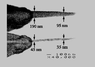
Figure 4. Electron-beam-deposited (EBD) tip for atomic force microscopy on top of a used conventional Silicon tip. The upper part shows the as-grown EBD tip, the lower part depicts the tip after a sharpening procedure.
C1. Fabrication and characterization of semiconductor nanostructures by atomic force microscopy
Non-destructive characterization of semiconductor nanostructures by atomic force microscopy (AFM) offers the possibility to get a deeper insight into the interaction of sample fabrication and the measurement of physical properties of these structures. Furthermore, the AFM is used for nanometer-scale lithography at ambient conditions by mechanically modifying a thin resist layer. Hereby the smallest feature size is determined by the tip radius. Best results are obtained with electron beam deposited tips, which are additionally sharpened in an oxygen plasma. At the moment we are able to write holes in photoresist with a period of 9 nm and a minimal structure size of 2 to 3 nm. Meanwhile we are able to directly pattern semiconductor layers by modified EBD-tips. On the other side, a special method of local anodic oxidation has been successfully developed. Here we are able to modify metals and semiconductors with a typical smallest structure size in the range of 10 nm. Current investigations aim at the characterization and optimization of the electrical properties of such oxides for possible device application.
C2. X-ray investigations of laterally structured surfaces
For a collaboration with M. Tolan and W. Press at Kiel University we fabricate surface gratings on silicon (period: 500 nm to 1000 nm; height: 1 nm to 20 nm) using holographic lithography followed by a dry etching process. Subsequently such gratings are covered with a thin deposit of different materials and studied by small-angle x-ray diffraction from this well defined surface roughness. For the case of SiGe deposited films the replication factor is extracted from the x-ray analysis. In a polystyrene-silicon system the interface interaction can be deduced from the diffraction measurements.
C3. Nanoscale 'Supertips' for AFM
The quality of atomic force microscope (AFM) micrographs crucially depends on the quality of the used tips. Under financial support of the Volkswagen-Stiftung and Neue Werkstoffe we have developed so called electron beam deposited (EBD) tips, which additionally can be sharpened in a special plasma etch process. This needle shaped tips are very sharp, extremely stable and chemically inert. We use this tips e.g. for high resolution topographic investigations of very deep, narrow trenches as well as for high resolution nanolithography. The feasability of these needle shaped, custom designed tips in biology, biophysics or colloid physics have been proved in a number of collaborations as e.g. with the Deutsches Krebsforschungsinstitut or the Max-Planck Institut für Kolloid und Grenzflächenphysik. The tips now are commercially available (NanoTOOLS GmbH) and are distributed by Digital Instruments. New developments as conductive EBD tips or test samples for AFM purpose are actually in development.
C4. Relaxation and Formation Dynamics of Wannier Excitons Studied by Spatiotemporal Pump and Probe Experiments
In collaboration with the group of Prof. Jochen Feldmann (Sektion Physik, University of Munich) we fabricate e-beam-lithographically defined gold structures on semiconductor quantum wells for spatial calibration purposes of femtosecond optical pump and probe experiments. The spatial resolution is in the order of 1 micron. Such spatiotemporal nonlinear optical experiments give important insight into the relaxation processes of 1s-excitons with non-vanishing in-plane center-of-mass momentum. We obtain picosecond transients of the ambipolar diffusion 'constant', which allow us to determine the temporal dynamics of formation, cooling and heating of 1s-excitons by varying the excess energy of the optically excited electron-hole pairs and the crystal temperature. We find an exciton formation time of 3 ps, exciton cooling due to acoustic phonon emission, and temperature dependent exciton heating rates governed by optical phonon scattering for temperatures higher than 50 K.
Guest Scientists, Visitors, and their Sponsors in 1996
- Prof. Valeri Dolgopolov (Institute of Solid State Physics, Chernogolovka,
Russia)
- Volkswagen Stiftung
- Prof. Alexander V. Chaplik (Inst. of Semiconductor Physics, Novosibirsk,
Russia)
- Volkswagen Stiftung
- Prof. Jim Allen (UC Santa Barbara, USA)
- Humboldt Research Awardee
- Prof. Sergio Ulloa (Ohio State University, USA)
- Humboldt Research Fellow
- Dr. Alexander O. Govorov (Inst. of Semiconductor Physics, Novosibirsk,
Russia)
- Humboldt Reserarch Fellow
- Dr. Mason Thomas (UC Santa Barbara, USA)
- EC-US Collaboration
- Dr. Thomas Kraft (Univ. Halle-Wittenberg)
- SFB 348
- Dr. Mathias Wagner (Hitachi Research Lab, Cambridge, UK)
- SFB 348
- Dr. Mike Wanke (UC Santa Barbara, USA)
- EC-US Collaboration
Diploma Theses completed in 1996
- Martin Streibl
"Kollektive Effekte in der Interminiband-Resonanz eines Halbleiter-Übergitters und der Intersubband-Resonanz undotierter Quantentöpfe" - Christoph Kadow
"Optische Anregungen in Quantentöpfen mit lateralen Potentialübergittern" - Markus Rotter
"Akustoelektrische und akustooptische Untersuchungen an GaAs/LiNbO3-Hybridsystemen" - Armin Tilke
"Dynamik des quantisierten Hall-Effektes: Absorption von akustischen Oberflächenwellen an AlSb/InAs/AlSb-Quantentöpfen" - Petra Denk
"Tunnelexperimente an parabolischen Quantentöpfen" - Markus Kehrle
"Lokale Oxidation mit einem Rasterkraftmikroskop" - Joao Cortes Rosa
"Magnetotransport in InAs-Oberflächenquantentöpfen mit quadratischen Modulationsübergittern" - Mark Haslinger
"Spektroskopie an gekoppelten GaAs/InAs-Quantendots"
Doctoral Theses completed in 1996
- Helmut Kriegelstein
"Untersuchungen zur Hochfrequenzankopplung an ballistischen Quantenpunktkontakten in Halbleiter-Heterostrukturen" - Martin Wendel
"Herstellung und Untersuchung von Halbleiterbauelementen mit dem Rasterkraftmikroskop"
Publications in 1996
A. Transport Properties
- 1-96
K. Ensslin, W. Hansen, and J. P. Kotthaus
"Electron Motion in Lateral Superlattices on Semiconductors"
in "Molecular Electronics", Eds. V. May, G. Mahler, and M. Schreiber (Dekker, New York 1996) pp. 143-170. - 2-96
K. Ensslin and R. Schuster
"Fabrication and Electronic Properties of Antidot Superlattices"
in "III-V Semiconductor Quantum Systems", Ed. K. Ploog (The Institution of Electrical Engineering, IEE, London 1996), pp. 102-138. - 3-96
F. Hofmann and D.A. Wharam
"Investigations of the Coulomb Blockade in a Parallel Quantum Dot Geometry"
in "Festkörperprobleme, Advances in Solid State Physics, Ed. R. Helbig (Vieweg, Braunschweig 1996) Vol. 35, pp. 197-213. - 4-96
T. Schlösser, K. Ensslin, J. P. Kotthaus, and M. Holland
"Internal Structure of a Landau Band Induced by a Lateral Superlattice: A Glimpse of Hofstadter's Butterfly"
Europhys. Lett 33, 683-688 (1996). - 7-96
D. Többen, D. A Wharam, G. Abstreiter, J. P. Kotthaus, and F. Schäffler
"Quantized Conductance in a Si/Si0.7Ge0.3 Split-Gate Device and Impurity-Related Magnetotransport Phenomena"
Solid State Electronics 40, 405-408 (1996). - 9-96
W. Hansen, D. Schmerek, and H. Drexler
"Quantum Wires and Quantum Dots in Heterojunction Devices with Field-Effect Electrodes"
Brazilian Journal of Physics 26, 110-122 (1996). - 12-96
J. P. Kotthaus
"Künstliche Halbleiter-Nanostrukturen - Billiard mit Elektronen"
Spektrum der Wissenschaft, Mai 1996, Heidelberg, 25-32. - 15-96
K. Ensslin and Ralf Schuster
"Antidot-Übergitter - Flippern mit Elektronen
Physik in unserer Zeit 27, VCH Verlagsgesellschaft, Weinheim, 1996/2, 84-89. - 20-96
V. T. Dolgopolov, A. A. Shashkin, G. V. Kravchenko, I. M. Mukhametzhanov, M. Wendel, J. P. Kotthaus, L. W. Molenkamp, and C. T. Foxon
"Giant Growth of Quantum Oscillations in an Inhomogeneous 2D Electron System"
JETP Lett. 63, 63-69 (1996). - 21-96
M. Holzmann, D. Többen, P. Baumgartner, G. Abstreiter, A. Kriele, H. Lorenz, and F. Schäffler
"Magnetotransport of Electrons in Arrays of Wires in Si/Si0.7Ge0.3 Heterostructures"
Surf. Sci. 361/362, 673-676 (1996). - 24-96
T. Schlösser, K. Ensslin, J. P. Kotthaus, and M. Holland
"Interplay of Landau Band Width and Band Separation in a Square Lateral Superlattice"
Surf. Sci. 362/362, 847-850 (1996) - 31-96
T. Schlösser, K. Ensslin, J. P. Kotthaus, and M. Holland
"Landau Subbands Generated by a Lateral Electrostatic Superlattice - Chasing the Hofstadter Butterfly -"
Semicond. Sci. Technol. 11, 1582-1585 (1996). - 32-96
Jörg P. Kotthaus, W. Hansen, and D. A. Wharam
"Electronic Interactions between Quantum Dots"
Physica B 227, 1-5 (1996) - 36-96
R. Kaiser, B. Irmer, M. Wendel, T. Schlösser, H. Lorenz, A. Lorke, K. Ensslin, J.P. Kotthaus, and A. Gossard
"Influence of pinned orbits and runaway trajectories on the magneto transport in antidot lattices with a 'diatomic' basis",
in 23rd International Conferene on "The Physics of Semiconductors", Vol 2,
Eds. M. Scheffler and R. Zimmermann,
(World Scientific, Singapore, 1996) pp. 1501-1504 - 42-96
JD. Schmerek, S.Manus, A.O. Govorov, W. Hansen, J.P. Kotthaus, and M.Holland
"Compressible and Incompressible Strips in a Narrow Electron Channel"
Phys. Rev. B 54, 13816-13820 (1996)
B. Intra- and Interband Spectroscopy
- 6-96
M. Hartung, A. Wixforth, K. L. Campman, and A. C. Gossard
"The Effect of Resonant Sublevel Coupling on Intersubband Transitions in Coupled Double Quantum Wells"
Solid State Electronics 40, 113-115 (1996). - 8-96
A. Lorke, J. P. Kotthaus, J. H. English, and A. C. Gossard
"Local Far-Infrared Spectroscopy of Edge States in the Quantum Hall Regime"
Phys. Rev. B 53, 1054-1057 (1996). - 10-96
C. Gauer, A. Wixforth, J. P. Kotthaus, B. Brar, and H. Kroemer
"Spin Phenomena in Intersubband Transitions"
Superlattices and Microstructures 19, 241-249 (1996). - 13-96
M. Hartung, A. Wixforth, K. L. Campman, and A. C. Gossard
"Intersubband Transition in Band Gap Engineered Parabolic Potential Wells"
Superlattices and Microstructures 19, 55-60 (1996) - 14-96
C. Wetzel, R. Winkler, M. Drechsler, B. K. Meyer, U. Rößler, J. Scriba, J. P. Kotthaus, V. Härle, and F. Scholz
"Electron Effective Mass and Nonparabolicity in Ga0.47In0.53As/InP Quantum Wells"
Phys. Rev. B 53, 1038-1041 (1996). - 16-96
R. J. Warburton, B. Brar, C. Gauer, A. Wixforth, J. P. Kotthaus, and H Kroemer
"Cyclotron Resonance of Electron-Hole Systems in InAs/GaSb/AlSb"
Solid State Electronics 40, 679-682 (1996). - 17-96
G. Blanke, A. Lorke, J. P. Kotthaus, J. H. English, A. C. Gossard, and P. M. Petroff
"Photon-Assisted Tunneling in Coupled Quantum Wells"
Solid State Electronics 40, 421-424 (1996). - 18-96
R. J. Warburton, C. Gauer, A. Wixforth, J. P. Kotthaus, B. Brar, and H. Kroemer
"Intersubband Resonances in InAs/AlSb Quantum Wells: Selection Rules, Matrix Elements and the Depolarization Field"
Phys. Rev. B 53, 7903-7910 (1996). - 19-96
R. J. Warburton, C. Gauer, A. Wixforth, J. P. Kotthaus, B. Brar, and H. Kroemer
"Collective Effects in the Intersubband Resonance of InAs/AlSb Quantum Wells"
Superlattices and Microstructures 19, 365- (1996) - 22-96
Th. Ihn, C. Gauer, F. Koch, and J. P. Kotthaus
"Anisotropy of the Conductivity in d-Doped Multilayers"
Surf. Sci. 361/362, 583-586 (1996) - 23-96
C. Gauer, M. Hartung, A. Wixforth, J. P. Kotthaus, B. Brar, and H. Kroemer
"Zero-Field Spin-Splitting in InAs/AlSb Quantum Wells"
Surf. Sci. 362/362, 472-475 (1996). - 25-96
K. F. Kaesen, A. Huber, H. Lorenz, J. P. Kotthaus, S. Bakker, and T. M. Klapwijk
"Quantum Oscillation of the Cyclotron Mass in Two-Dimensional Electron Systems in Silicon"
Phys. Rev. B 54, 1514-1517 (1996). - 26-96
V. T.Dolgopolov, A. A. Shashkin, A. V. Aristov, D. Schmerek, H. Drexler, W. Hansen, J. P. Kotthaus, and M. Holland
"Nonlinear Screening in Two-Dimensional Electron Systems"
Physics of Low-Dimensional Structures 6, 1-22 (1996). - 27-96
W. Hansen and H. Drexler
"Spectroscopy on Field-Effect Induced Quantum Wires and Quantum Dots"
in "Festkörperprobleme, Advances in Solid State Physics, Ed. R. Helbig (Vieweg, Braunschweig 1996) Vol. 35, pp. 81-101. - 28-96
A. P. Förster, W. Hansen, A. Schmeller, J. P. Kotthaus, W. Klein, G. Böhm, G. Tränkle, and G. Weimann
"Modulation-Assisted Raman Scattering of Plasmons in Field-Effect Induced Potential Superlattices"
in "Highlights of Light Spectroscopy on Semiconductors", Eds. A. D'Andrea and L. G. Quagliano (World Scientific, Singapore 1996), pp. 183-186. - 29-96
M. Fricke, A. Lorke, J. P. Kotthaus, G. Medeiros-Ribeiro, and P. M. Petroff
"Shell Structure and Electron-Electron Interaction in Self-Assembled InAs Quantum Dots"
Europhys. Lett. 36, 197-202 (1996). - 33-96
A. O. Govorov, W. Hansen, and J. P. Kotthaus
"Voltage-Tunable Bragg Reflector Based on the Quantum Confined Stark Effect"
J. Appl. Phys. 80, 1-3 (1996). - p 19-96
JF.R. Frank, A.O. Govorov, W. Hansen, J.P. Kotthaus, and M. Holland
"New plasmon mode in coupled quantum wires in high magnetic fields"
Proceedings of 12th International Conference on the Application of High Magnetic Fields (Germany, 1996), World Scientific, in press.
C: Nanometer Fabrication and Characterization
- 5-96
M. Wendel, H. Lorenz, J. P. Kotthaus, and M. Holland
"Magneto Transport on Antidot Arrays Fabricated by an Atomic Force Microscope"
Solid State Electronics 40, 25-28 (1996). - 11-96
M. Tolan, G. Vacca, S. K. Sinha, Z. Li, M. H. Rafailovich, J. Sokolov, H. Lorenz, and J. P. Kotthaus
"Si/Ge Films on Laterally Structured Surfaces: An X-Ray Study of Conformal Roughness"
Appl. Phys. Lett. 68, 191-193 (1996). - 30-96
M. Wendel, B. Irmer, J. Cortes, H. Lorenz, J. P. Kotthaus, and A. Lorke
"Nanolithography with an Atomic Force Microscope"
Superlattices and Microstructures 20, 349-356 (1996).
Invited Talks in 1996
- T. Schlösser
" An experimental glimpse at the Hofstadter butterfly
Edgar-Lüscher-Seminar "Modern Aspects of Solid State Physics"
(Serneus, Switzerland, 1996) - J. P. Kotthaus
"Landau Subbands Generated by a Lateral Electrostatic Superlattice - Chasing the Hofstadter Butterfly", 9th Int. Winterschool "New Developments in Solid State Physics"
(Mauterndorf, Austria, 1996) - A. Lorke
"Far-Infrared spectroscopy of Self-Organized InAs/GaAs Quantum Structures"
Int. Workshop on Semiconductor Growth, Surface Morphology, and Quantum Phenomena
(Ringberg, Germany, 1996) - K. Ensslin
"Quantum Transport in Lateral Superlattices"
15th Gen. Conf. Condensed Matter Division of the European Physical Society ( Baveno Stresa, Italy, 1996) - K. Ensslin
"Lateral Superlattices: Classical Chaos, Phase Coherent Electrons and Artificial Bandstructure"
17th Nordic Semiconductor Meeting ( Trondheim, Norway, 1996) - D. A. Wharam
>Transport Properties of Coupled Quantum Dot Systems<
International Conference on Quantum Devices and Circuits
(Alexandria, Egypt, 1996) - M. Wendel
"AFM-Lithography"
3rd European Canadian Mesoscopic Initiative (ECAMI) Workshop
(Ottawa, Canada, 1996) - A. Wixforth
"Spin effects in the intersubband resonance of semiconductor quantum wells"
ICPS XXIII (Berlin, Germany, 1996) - A. Lorke
"Far-Infrared and Capacitance Spectroscopy of Self-Assemled InAs Quantum Dots"
23rd Int. Symp. "Compound Semiconductors" (St. Petersburg, Russia, 1996) - K. Ensslin
"Lateral Superlattices: Classical Chaos, Phase Coherent Electrons and Artificial Bandstructure"
XXXI. Rencontre de Moirond on "Correlated Fermions and Transport in Mesoscopic Systems"
Les Arcs, France, 1996 - K. Ensslin
"From Classical Chaos to Quantum Behavior: Electron Transport in Lateral Superlattices"
Adriatico Research Conference "Mesoscopic Phenomena in Complex Quantum Systems"
(Triest, Italy, 1996)
Financial Support:
Funding of this work via the following agencies is gratefully acknowledged:
- Deutsche Forschungsgemeinschaft
- Volkswagen-Stiftung
- Bundesministerium für Bildung und Wissenschaft, Forschung und Technologie (BMBF)
- Bayerische Forschungsstiftung FOROPTO
- Alexander von Humboldt - Stiftung
- European Community Project ESPRIT and HCM
- German - Israeli - Foundation
- Siemens AG München