

Research report 1995
Overview
Most of the modern electronic devices as used in state-of-the-art complex circuits like microprocessors etc. are nowadays based on so-called quasi-two-dimensional electron systems (Q2DES). Such Q2DES can be realized at the interface between a semiconductor and an insulator, or at the interface between two semiconductors.
In a Q2DES, the electrons are confined along one spatial direction to within a length scale comparable to their quantum-mechanical wavelength. In the plane perpendicular to the direction of the confinement, however, they are more or less free to move.
Apart from a much better defined switching behavior and less power consumption as compared to many bulk-based semiconductor devices, the interface- and Q2DES- based devices also offer insight into many new and fascinating physical properties which are related to the reduced dimensionality.
Modern semiconductor physics concentrates on a further reduction of the dimensionality of the electron systems under investigation. Nowadays, so-called quantum wires (or quasi-one-dimensional electron systems Q1DES) and even quantum dots (Q0DES) can be realized. Here, the motion of an electron as confined in the repective artificial potential well is additionally quantized into a series of eigenstates. For quantum dots, this complete quantization is very similar to the one of the electron in an atom - this is why quantum dots are sometimes referred to as 'artificial atoms'. However, unlike to their real counterparts, the number of electrons per artificial atom may be tuned externally by, e.g. an electric field. Thus - we expect something like a revival of atomic physics if we continue to follow this tremendously interesting path.
In our research group here at the LMU, we study the properties of such electron systems which are confined to very small dimensions to form Q2DES, Q1DES and Q0DES as well as interactions between those low-dimensional systems. Also, the fundamental technologies to produce such systems are investigated and exploited. We concentrate on semiconductor structures based on the Si/SiO2 as well as compound semiconductor combinations such as GaAs/AlGaAs, InAs/AlSb, InAs/GaAs and related heterojunctions. Our work is based on several close collaborations with groups around the world that grow and characterize the above listed heterostructures with highest quality. Using different sophisticated facilities in our cleanroom lab we are able to laterally pattern the semiconductor structures down to lengthscales of only a few nanometers. We apply different lithografic techniques, such as holography, electron beam writing, and atomic force microscopy, which allow for a very flexible realization of very small sample sizes.
Experimentally, our setups provide the more or less unique opportunity to investigate our samples over a very wide frequency range from DC up to the UV region. We have access to several different high frequency setups (DC..20 GHz), a microwave vector network analyzer (8.5GHz..350 GHz), an (far-)infrared molecular laser, two (far-)infrared Fourier Transform Spectrometers and different laser systems, some of which are tuneable from the near infrared into the visible spectral range. All of our experimental setups are equipped with low-temperature cryostats and superconducting magnet systems, providing magnetic fields up to 15 Tesla. The combination of all our equipment and experimental facilities provides us with the basis for a detailed investigation of the new physical properties of semiconductor nanostructures.
A. Transport Properties
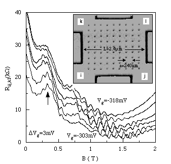
Figure 1. Magnetoresistance traces of a finite antidot lattice at T= 30 mK at very low carrier densities. The arrow indicates the classical commensurability maximum. The inset shows an image taken with an atomic force microscope of a wet-etched surface of a GaAs/AlGaAs- heterostructure with the characteristic dimensions as indicated. Ohmic contacts are made to the corners of the square indicated by i,j,k and l.
A.1. Interaction of Surface Acoustic Waves (SAW) and Low-Dimensional Electron
Systems
Surface acoustic waves are modes of elastic energy which can propagate on the surface of different materials. If the substrate is piezoelectric, those waves are accompanied by electric fields which then propagate at the speed of sound. The electric fields of the wave can couple to the mobile carriers within a semiconductor structure and modify its electronic and elastic properties. By measuring the attenuation of the wave and the renormalization of the sound velocity we can, for instance, extract information on the dynamic conductivity of the electron system. We also investigate the possibility to use a SAW for a dynamical lateral potential modulation and we investigate the influence of a SAW onto the optical properties of an electron system. Our experiments presently cover the frequency range between 100 MHz and 6 GHz, corresponding to surface acoustic wavelengths between 30um and 0.5um, respectively. Potential device applications combining acousto-electric and acousto-optical effects are another research topic under this headline.
A.2. Capacitance Spectroscopy on Single Field-Effect-Induced Electron Wires
in AlGaAs-GaAs Heterostructures
In specially designed heterostructure crystals grown by M. Holland in Glasgow we use e-beam defined gate electrodes to generate 150mm long quantum wires with different widths. We perform capacitance spectroscopy to investigate the electronic properties of very high quality electron wires. Because of the very small capacitance involved we developped a capacitance bridge with an impedance transformer close to the sample.
In the case of broad electron channels (width ~300nm) at high magnetic fields we find a good qualitative agreement with a model by A. O. Govorov, that considers the contribution of edge channels to the capacitance signal in the quantum-Hall regime. In the case of narrow wires (width <100nm) we find that the length scale of fluctuations that cause broadening of the capacitance spectra is smaller than 150mm. In strong confinement potentials the resistive signal indicates an impeded charging at higher subband occupation that becomes more pronounced in high magnetic fields.
A.3. Coulomb Blockade Phenomena in Quantum Dots
The transport properties of quantum dot structures at low and ultra-low temperatures are governed by so-called single-electron-effects. The number of electrons being present in such a dot structure is quantised in units of the elementary charge e : This fact together with the very small capacitance of the dot leads to the occurence of the so-called Coulomb blockade effect which can be systematically studied using transport experiments at low temperatures. On high mobility GaAs/AlGaAs heterojunctions grown at the Walter Schottky Institut of the TU München we fabricate fine gate patterns with e-beam lithography that enable us to electrostatically define quantum point contacts and quantum dots. We investigate electronically tuneable quantum dots and also coupled quantum dot systems. A further tool to understand the nature of single-electron effects is an external magnetic field. The influence of this external magnetic field onto the internal electronic structure of the dot is investigated in great detail. The self-consistent density distribution within the dot structure leads to a pronounced modification of the Coulomb blockade effects which can be understood in terms of a magnetic filed dependent phase diagram. Similar phase diagrams are used to describe the internal structure and Coulomb blockade effects in coupled double dot systems.
A.4. High Frequency Properties of Quantum Point Contacts and Quantum Dots
The non-linear transport properties of ballistic quantum point contacts are investigated and well understood nowadays. We employ these non linearities in the IV characteristic of ballistic point contacts to aim towards a high frequency signal processing. First experiments using ballistic point contacts as high frequency mixers are very promising in these terms. We develop techniques to efficiently couple high frequency radiation into the ballistic point contact by using lenses, antennae and multi point contact arays.
A.5. Quantum Transport in Lateral Superlattices
Classical commensurability oscillations in the magneroresistance caused by the
commensurability of the classical cyclotron diameter and the period of a man-made
lateral superlattice have been extensively studied and are now well understood. This
year we succeeded in observing quantum commensurability effects between the magnetic
flux per unit cell of the lattice and the magnetix flux quantum: If there are p/q
flux quanta per unit cell the Landau bands are predicted to split into p subbands.
This effect is visualized in the famous "Hofstadter Butterfly". On very
homogeneous modulation-doped GaAs/AlGaAs heterostructures with a shallow 2DES grown
by M. Holland in Glasgow we fabricated corrugated
gates with e-beam lithography which allow us to field-effect induce square lateral
superlattices with periods between 140nm and 80nm. Tuning carefully the superlattice
potential amplitude as well as the magnetic field our experiments demonstrates that
it is possible to observe at very low temperatures this subband splitting as a splitting
of Shubnikov-de Haas oscillations. The experiment reveals also the strong influence
of many body effects on the resulting subbband structure.
A.6. Electronic Phase Transition in Two-Dimensional Electron Systems
In a close collaboration with the group of V. Dolgopolov at the Russian
Academy of Sciences in Chernogolovka we study the metal insulator transition
in the quantum Hall effect regime by analysing the magneto-transport properties at
low temperatures in specially designed sample geometries. In current-voltage experiments
on samples with Corbino geometry we find that the characteristica of all insulating
phases in the integer and fractional quantum Hall regime are very similar and can
be well understood as resulting from a percolation metal insulator transition. Recently
we extended our transport studies to samples with intentionally induced inhomogeneities
of the electron density. In MISFET-type heterojunctions we also investigate the low-frequency
admittance between a back contact and the 2DES. At integer Landau level filling factors
we find signatures of a Coulomb gap in the tunneling density of states.
A.7. Transport through Nanostructures on Si-Ge
Improvements in the quality of MBE-grown SiGe material have recently prompted much interest in this material system and related Si-SiGe heterostructures. Mobilities as high as 200000 cm^2/Vs have been reported and the low-temperature mean free paths are such that ballistic effects can now be readily investigated. In collaboration with the Walter Schottky Institut of the TU München we have undertaken initial experiments on the physics of mesoscopic devices in SiGe heterostructures. In particular the conductance quantisation first observed in GaAs-AlGaAs heterostructures has been studied in quantum point-contacts defined in this system. Interestingly the observed steps in the conductance are quantised in units of 4e^2/h due to the additional valley degeneracy. The shorter mean free path leads to a more pronounced influence of the individual impurities upon the conductance quantisation and these effects have been systematically investigated.
B. Intra- and Interband Spectroscopy
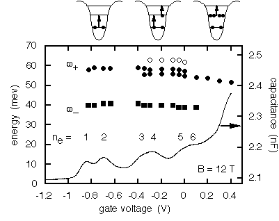
Figure 2. Far-infrared transition energies w+ and w# of self-assembled quantum dots at B = 12 T as a function of gate voltage (left scale). The number of occupied electron states, ne, as deduced from the CV trace (solid line, right scale) is indicated. The inset shows possible transitions for 2, 3, and 6 electrons per dot.
B.1. Electron Systems in Band Gap Engineered Quantum Systems
Modern crystal growth techniques like molecular beam epitaxy nowadays offer the unique advantage of tailoring the band edges of different semiconductor systems in a very controlled manner. A prominent example is the so-called parabolic quantum well (PQW), but also more complex systems can be realized.
In close co-operation with the research group of A.C. Gossard in Santa
Barbara we concentrate on the investigation of the collective reponse of low-dimensional
electron systems in such man-made semiconductor structures. As an example, the electron
system in the parabolic quantum well represents in good approximation the concept
of a free electron system in a homogenous positive background ('JELLIUM'). We show
that this electron system on the one hand can be understood as an approach towards
a highly mobile quasi-three dimensional electron system. On the other hand, however,
the parabolic confinement potential offers many unique features, which can be understood
as close analogies to the physics of quantum wires and dots. Using sophisticated
experimental techniques we could illucidate many of the physical properties of also
those nanostructures using the PQW approach.
Recently, we also focused on the investigations of the properties in coupled quantum
well structures on the basis of PQW. Here, too, the very precise control of the potential
profiles in growth direction can be used to fabricate nearly any desired structure.
For instance, in analogy to the term 'artificial atom' we study the properties of
artificial 'molecules' using two coupled PQW as a simple but powerful model system.
B.2. Physics and Technology of Quantum Wells with Narrow Gap Semiconductors
The relatively small energy gap of some semiconductors like InAs and the related pronounced coupling of neighbouring bands leads to strong non-parabolic effects in the energy vs. momentum dispersion relation. Such a non-parabolicity reflects, e.g., in a strongly energy dependent effective mass. To study such effects we concentrate on a relatively new material combination, namely InAs/AlSb which also provides the deepest quantum wells available to date.
The investigation of the transitions between two electrical subbands in this quantum well system reveals most of the fundamental properties of the band structure. By application of a special spectroscopic technique we were able to not only excite spin-conserving but also spin flip intersubband transitions. Moreover - we could show that in this material combination the inversion asymmetry of the host crystalresults in a strong zero magnetic field spin-splitting.
Collective effects on the intersubband resonance in quantum wells are also being studied using the InAs/AlSb system, following our observation that the resonance is drastically narrowed as compared to the single particle spectrum. We now understand this as a consequence of the depolarisation field. Further experiments are underway to probe the role of the boundary conditions at the InAs/AlSb interfaces, to study the possible couplings between the 1-2 and 2-3 transitions, and to investigate the physics of a metal grating used to excite the resonance. An analogous collective effect arises in a superlattice when electrons are excited from the first to the second miniband and this is being probed experimentally with high-mobility superlattices, grown by embedding a superlattice in a parabolic well.
Not only from the physics point of view this material combination is a very attractive candidate for semiconductor research. The unique band structure together with high carrier concentrations and small effective masses makes it very interesting for possible device applications. Here, we focus on the photonic properties and the optoelectronic response. Possible applications include infrared detectors, modulators, and switches in the infrared regime. In close co- operation with the research group of H. Kroemer at UC Santa Barbara (USA) we design and develop suitable layer structures to follow this route.
B.3. Magnetoplasmons in Quantum Dots and Wires
We investigate magnetoplasmon excitations of laterally confined Q1DES and Q0DES by measuring the microwave and far-infrared absorption of these collective modes in high magnetic fields and at low temperatures. One focus of recent work has been the study of edge magnetoplasmons on a single electron disc to eliminate the effects of inhomogeneous broadening that can occur in array-type samples consisting of many nominally identical mesoscopic objects. Another focus has been the investigation of quantum wire superlattices with a unit cell containing two closely separated wires. Here the electron channels with variable electron density are induced by field effect in a GaAs/AlAs MIS structure. In the transition region from size to magnetic quantization we observe several magnetoplasma modes which show similar behaviour as has been observed in single quantum wire lattices with nonparabolic bare confinement potential. In high magnetic fields (over 5 T) we observe two modes. In a classical model, we can associate the lower energy resonance with a charge transfer across the barrier between the two channels and the higher energy resonance with a charge fluctuation in the individual channels. The oscillator strength distribution among the two resonances depends on the height of the barrier between the channels that is strongly influenced by the charge distribution on the free GaAs surface between the gate strips under which the quantum wires are induced. Hence the measurements allow us to examine the behaviour of the surface charges under different conditions.
B.4. Influence of Infrared Excitation on the Low-Frequency Transport in Low-Dimensional Systems
The combination of DC transport and (far)-infrared excitation experiments offers a number of interesting opportunities. In these experiments, e.g., the sample itself serves as a detector, which is not only interesting from a technological point of view but also offers the advantage of local detection, which is of great benefit especially for samples which are smaller than the wavelength of the excitation radiation. Using this technique, we have investigated the dynamics of edge states in the quantum Hall effect. Because of very low scattering, these edge channels are in a way ideal one-dimensional model systems. However, spectroscopy on these channels proves to be extremely difficult because of the fact that they are strips of only ~ 0.5 um next to a much larger area of two-dimensional electron gas which absorbs in the same frequency regime. Using the edge channels as detectors, together with employing a micro-shadow mask technique, we were able to detect different excitations of quantum Hall edge states and obtain information on the local curvature of the edge potential in etched and gated Hall bars.
Another experiment which combines infrared excitation and DC transport was performed on selectively contacted coupled double quantum wells. Either through a special growth technique or using front- and back-gating pinch-off, quantum wells which are only ~ 10 nm separated from each other can individually be contacted. The tunneling resistance between the wells is then given by the overlap of the wavefunctions of the wells, which is expected to be larger for excited states than for the ground state. Therefore, infrared excitation, which pumps electrons into higher states, is expected to result in an increased tunneling current. Different tunneling structures were realized and an infrared-radiation-induced increase of the tunneling current was observed, giving first evidence of photon-assisted tunneling of electrons through the barrier between coupled double quantum wells.
B.5. Spectroscopy of Self-Organized InAs Quantum Dots
With decreasing sizes of nanostructures the problem of homogeneity becomes more and more important. Ideally, one would like to study large arrays of identical quantum systems. One elegant way to achieve this is to use fabrication mechnisms where the shape and the dimensions of the nanostructures are given by, energetic considerations, such that energy minimization will lead to the desired sample homogeneity. This happens, e.g. in the Stranski-Krastanow growth mode of InAs on GaAs heteroepitaxy and results in layers of uniform quantum dots of ~ 20 nm diameter and ~ 7 nm height. In a close collaboration with the group of P. Petroff at UC Santa Barbara we have demonstrated that these dots can be integrated into a metal-insulator-semiconductor heterostructure, which allows us to tune the electron number per dot, determine it by capacitance spectroscopy, and study the dots' excitation in the far-infrared. Here, the far-infrared spectroscopy resembles the atomic spectroscopy mentioned in the introduction. Indeed, we can "tune the dots through the table of elements" and distinguish, e.g. "quantum dot Helium" and "quantum dot Lithium" by their excitation spectrum. Furthermore, we can directly compare the different ground states of these few-electron systems, and, from a comparison between ground state and excitation energies, derive detailed information on the Coulomb and quantization contributions to the energetic structure of these man-made atoms.
B.6. Optically Detected Resonances
There are advantages of measuring the far infra-red properties of carriers excited by an above band gap laser beam. These include the ability in principle to measure completely undoped samples, the possibilitiy to study excitons (rather than free carriers) in various potentials, and to perform local far infra-red spectroscopy where the sample size is determined by the visible laser beam. Hence, an experiment has been set up whereby a Fourier transform spectrometer has been coupled with near infra-red optics using optical fibre technology. Experiments are planned on the intersubband resonance of various quantum well systems and on self-assembled quantum dots.
B.7.Optics on Field-Effect Induced Tuneable Potential Superlattices in AlGaAs-GaAs Heterostructures.
By means of two interdigital transducer gates on a AlGaAs-GaAs heterostructure we induce a widely tuneable lateral potential type II superlattice of period d=500nm. Furthermore, by applying a votage between the two transducers and a back contact we can create a two-dimensional charge density modulated electron system in the plane of the GaAs quantum well or an array of one-dimensional electron channels. This was confirmed by plasmon excitations of the electron system in resonant inelastic light scattering experiments. In the case of an unloaded empty quantum well the Quantum Confined Stark Effect and the lateral Franz-Keldysh Effect account for the observed optoelectronic properties. At moderate superlattice potential amplitudes photo- induced excitons are localised in one-dimensional regions of maximum vertical electric fields; at higher superlattice potential amplitudes they are ionised due to strong lateral electric fields. We are presently studying the effect of a strong vertical magnetic field on our system and we are searching for spatially indirect transitions in the superlattice. A further aim is to perform time and spatially resolved measurements of exciton diffusion.
C: Nanometer Fabrication and Characterization
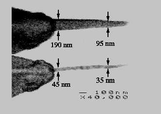
Figure 3. Electron-beam-deposited (EBD) tip for atomic force microscopy on top of a used conventional Silicon tip. The upper part shows the as-grown EBD tip, the lower part depicts the tip after a sharpening procedure.
C.1. Fabrication and Characterization of Semiconductor Nanostructures by Atomic Force Microscopy
Non-destructive characterization of semiconductor nanostructures by atomic force microscopy (AFM) offers the possibility to get a deeper insight into the interaction of sample fabrication and the measurement of physical properties of these structures. Furthermore, the AFM is used for nanometer-scale lithography at ambient conditions by mechanically modifying a thin resist layer. Hereby the smallest feature size is determined by the tip radius. Best results are obained with electron beam deposited tips, which are additionally sharpened in an oxygen plasma. At the moment we are able to write strctures into a photoresist layer with a period of 9 nm and a minimal structure size of 2 to 3 nm.
C2. X-Ray Investigations of Laterally Structured Surfaces
For a collaboration with M. Tolan and W. Press at Kiel University we fabricate surface gratings on silicon (period: 500 nm to 1000 nm; height: 1 nm to 20 nm) using holographic lithography followed by a dry etching process. Subsequently such gratings are covered with a thin deposit of different materials and studied by small-angle x-ray diffraction from this well defined surface roughness. For the case of SiGe deposited films the replication factor is extracted from the x- ray analysis. In a polystyrene-silicon system the interface interaction can be deduced from the diffraction measurements.
Guest Scientists, Visitors, and their Sponsors in 1995
- Prof. Alik Chaplik (Inst. of Semiconductor Physics, Novosibirsk, Russia)
- Volkswagen Stiftung
- Prof. Valeri Dolgopolov (Semiconductor Institute, Chernogolovka, Russia)
- Volkswagen Stiftung, and SFB 348
- Dr. Matvei Entin (Inst. of Semiconductor Physics, Novosibirsk, Russia)
- Volkswagen Stiftung
- Dr. Kenichi Fujii (College of General Education Osaka University)
- SFB 348
- Dr. Alexander O. Govorov (Inst. of Semiconductor Physics, Novosibirsk,
Russia)
- Volkswagen Stiftung , and SFB 348
- Dr. Gilberto Medeiros-Ribeiro (UC Santa Barbara, USA)
- EC-US Collaboration
- Prof. Pierre Petroff (UC Santa Barbara, USA)
- Humboldt Research Awardee
- Dr. Frank Stern (IBM Yorktown Heights, USA)
- Humboldt Research Awardee
- Prof. Sergio Ulloa (Ohio State University, USA)
- Humboldt Research Fellow
Diploma Theses completed in 1995
- Andreas Berger
"Dynamische Leitfähigkeit von Elektronensystemen mit parabolischem Einschlußpotential" - Gerd Blanke
"Intersubbandresonanz-Detektion in gekoppelten AlGaAs-Quantentöpfen" - Carsten Dörrhöfer
"Design und Realisierung einer Photodiode aus InGaAs/InP für eine Übertragungsrate von 40 Gbit/s" - Andreas Förster,
"Ramanstreuung an Plasmonen in lateral modulierten Quantentöpfen" - Michael Fricke
"Kapazitäts- und Fourierspektroskopie an InGaAs Quantendots" - Wolfgang Frank,
"Magnetoplasmonen in Quantendrahtübergittern mit komplexer Einheitszelle" - Alexander Haubrich,
"Mischexperimente an angepaßten parallelen Quantenpunktkontakten" - Ralf Kaiser
"Magnetotransportuntersuchungen an kraftmikroskopisch hergestelltem Antidot- Übergittern mit "zweiatomarer" Basis" - Alexander Marseille
"Optische Untersuchungen an parabolischen Einfach- und Mehrfachquantentöpfen" - Peter Müller
"Bestimmung der dynamischen Leitfähigkeit niedrigdimensionaler Elektronensysteme mit akustischen Oberflächenwellen" - Stefan Reinig,
"Kopplungsphänomene bei Transportuntersuchungen an Quantenpunkten" - Dieter Schmerek,
"Kapazitätsspektroskopie an niedrigdimensionalen Elektronensystemen" - Simon Wagner
"Laterale Strukturierung von InAs/AlSb- Quantentöpfen"
Doctoral Theses completed in 1995
- Christoph Gauer
"Intersubbandresonanz und Spinphänomene in zweidimensionalen Elektronensystemen" - Till Schlösser
"Quantentransport in lateralen Übergittern"
Habilitations in 1995
- David Wharam,
"Ladungsquantisierung und Kohärenzphänomene in Quantenpunkten und Quantenpunktkontakten"
Publications in 1995
A. Transport Properties
- W. Hansen, D. Schmerek, and H. Drexler
"Quantum Wires and Quantum Dots in Heterojunction Devices with Field-Effect Electrodes"
Brazilan Journal of Physics 26, 110 (1996) - Jörg P. Kotthaus, W. Hansen, and D. A. Wharam
"Electronic Interactions between Quantum Dots"
Physica B, in press - J. P. Kotthaus
"Flipper-Automaten für Elektronen ?"
Einsichten 1, 1995 (LMU München 1995) - D. A. Wharam and T. Heinzel
"Coulomb Blockade in Quantum Dots"
Proc. of ICTP-NATO Workshop on "Submicron Quantum Dynamics", Trieste 1994,
in press - F. Hofmann, T. Heinzel, D. A. Wharam, J. P. Kotthaus, G. Böhm, W. Klein,
G. Tränkle, and G. Weimann
"Single Electron Switching in a Parallel Quantum Dot"
Phys. Rev. B 51, 13872-13875 (1995). - T. Heinzel, F. Hofmann, D. A. Wharam, J. P. Kotthaus, G. Böhm, W. Klein,
G. Tränkle, and G. Weimann
"Modulation of Coulomb-Blockade Oscillations by Coherence and Quantisation Effects"
"The Physics of Semiconductors", Vol. 3, Ed. David J. Lockwood, (World Scientific , Singapore, 1995) pp. 1871-1 - F. Hofmann and D.A. Wharam
"Investigations of the Coulomb Blockade in a Parallel Quantum Dot Geometrie"
Festkörperprobleme 35 (Vieweg, Braunschweig, 1995), in press - K. Fujii, W. Gödel, D. A. Wharam, S. Manus, J. P. Kotthaus, G. Böhm,
W. Klein, G. Tränkle, and G. Weimann
"Microwave Modulation of Coulomb-Blockade Oscillations in a Quantum Dot"
Physica B, in press - K. Ensslin, W. Hansen, and J. P. Kotthaus
"Electron Motion in Lateral Superlattices on Semiconductors"
in "Molecular Electronics", Eds. G. Mahler, V. May, and M. Schreiber (Dekker, New York, 1996) pp 143-170 - R. Schuster, K. Ensslin, D. A. Wharam, V. T. Dolgopolov, J. P. Kotthaus, G. Böhm,
W. Klein, G. Tränkle, and G. Weimann
"Phase-Coherent Electrons Travelling along Classical Electron Trajectories"
"The Physics of Semiconductors", Vol. 3, Ed. David J. Lockwood, (World Scientific , Singapore, 1995) pp. 1979-1986 - T. Schlösser, K. Ensslin, F. Claro, J. P. Kotthaus, M. Holland, and R. Ketzmerick
"Corrugation-Induced Transverse Voltage in a Lateral Superlattice"
Phys. Rev. B51, 10737 (1995) - K. Ensslin and R. Schuster
"Antidot Superlattices: Classical Trajectories and Phase Coherent Electrons"
"Quantum Dynamics of Submicron Structures", Eds. Hilda A Cerdeira, Bernhard Kramer, and G. Schön, NATO ASI Series, Vol. 291 (Kluwer Academic Publishers, Netherlands, 1995) p. 247-261 - R. Schuster, K. Ensslin, V. Dolgopolov, J. P. Kotthaus, G. Böhm, and W. Klein
"Edge State Transport in Finite Antidot Lattices"
Phys. Rev. B52, 14699 (1995) - R. Schuster, K. Ensslin, D. Wharam, V. Dolgopolov, J. P. Kotthaus, G. Böhm,
W. Klein, G. Tränkle, and G. Weimann
"Quantum Interference Effects in Finite Antidot Lattices"
Inst. Phys. Conf. Ser. 141, 831-834 (1995) - P. Denk, T. Schlösser, and K. Ensslin
"Experimental Control of the Number of Ionized Donors in an AlGaAs/GaAs Heterostructure"
Acta Physica Polonica A88, 977 (1995) - T. Schlösser, K. Ensslin, J. P. Kotthaus, and M. Holland
"Interplay of Landau Band Width and Band Separation in a Square Lateral Superlattice"
Surface Science, in press - K. Ensslin, R. Schuster, and T. Schlösser
"Lateral Superlattices: Classical, Semi-Classical, and Quantum Mechanical Transport Phenomena"
Proc. of the NATO ASI "Frontieres in Nanoscale Science of Micron/Submicron Devices", Kiev, Ukraine, 1995, in press - V. T. Dolgopolov, H. Drexler, W. Hansen, J. P. Kotthaus, and M. Holland
"Electron Correlations and Coulomb Gap in a Two-Dimensional Electron Gas in High Magnetic Fields"
Phys. Rev. B 51, 7958 (1995) - V. T. Dolgopolov, A. A. Shashkin, G. V. Kravchenko, I. M. Mukhametzhanov, M. Wendel,
J. P. Kotthaus, L. W. Molenkamp, and C. T. Foxon
"Giant Growth of Quantum Oscillations in an Inhomogeneous 2D Electron System"
JETP Letters 63, 55 (1995) - M. Holzmann, D. Többen, M. Wendel, H. Lorenz, G. Abstreiter, J. P. Kotthaus,
and F. Schäffler
"One-Dimensional Transport of Electrons in Si/Si0.7Ge0.3 Heterostructures"
Appl. Phys. Lett. 66, 833-835, (1995). - D. Többen, D. A. Wharam, G. Abstreiter, J. P. Kotthaus, and F. Schäffler
"Ballistic Electron Transport through a Quantum Point-Contact Defined in Si/SiGe Heterostructures"
Semicond. Sci. Technol., in press - D. Többen, D.A. Wharam, G. Abstreiter, J.P. Kotthaus, and F. Schäffler
"Transport Properties of a Si/SiGe Quantum Point-Contact in the Presence of Impurities"
Phys. Rev. B52, 4704 (1995) - D. Többen, D. A Wharam, G. Abstreiter, J. P. Kotthausd, and F. Schäffler
"Quantized Conductance in a Si/Si0.7Ge0.3 Split-Gatee Device and Impurity-Related Magnetotransport Phenomena"
Solid State Electronics, in press
B. Intra- and Interband Spectroscopy
- M. Hartung, A. Berger, A. Wixforth, P. F. Hopkins, J. H. English, and A. C. Gossard
"Quantum Interference Effects in the Collective Response of Asymmetric Coupled Quantum Wells"
"The Physics of Semiconductors", Vol. 2, Ed. David J. Lockwood, (World Scientific , Singapore, 1995) pp. 1087-1090 - M. Hartung, A. Wixforth, K.L. Campman, and A.C. Gossard
"Intersubband Transitions in Bandgap-Engineered Parabolic Potential Wells"
Superlattices and Microstructures, 1996, vol.19, (no.1):55-60 - M. Hartung, A. Wixforth, K. L. Campman, and A. C. Gossard
"The Effect of Resonant Sublevel Coupling on Intersubband Transitions in Coupled Double Quantum Wells"
Solid State Electronics, in press - A. Wixforth, M. Hartung, K. L. Campman, and A. C. Gossard
"Collective Excitation in Single and Double Parabolic Quantum Wells"
Physics of Low-Dimensional Structures 10/11, pp.87-104 (1995) - C. Gauer, J. Scriba, R.J. Warburton, A. Wixforth, J.P. Kotthaus, C.R. Bolognesi,
C. Nguyen, B. Brar, and H. Kroemer
"Cyclotron Resonance in InAs/AlSb Quantum Wells"
"The Physics of Semiconductors", Vol. 1, ed. David J. Lockwood, (World Scientific, Singapore 1995), pp. 739-741 - C. Gauer, A. Wixforth, J. P. Kotthaus, G. Abstreiter, G. Weimann, and W. Schlapp
"Magnetic-Field-Induced Intersubband Resonances in AlGaAs/GaAs Quantum Wells"
Europhysics Letters 30, 111 (1995) - R. J. Warburton, C. Gauer, A. Wixforth, J. P. Kotthaus, B. Brar, and H. Kroemer
"Collective Effects in the Intersubband Resonance of InAs/AlSb Quantum Wells"
Superlattices and Microstructures, in press - C. Gauer, A. Wixforth, J. P. Kotthaus, M. Kubisa, W. Zawadzki, B. Brar, and H.
Kroemer
"Magnetic-Field-Induced Spin-Conserving and Spin-Flip Intersubband Transistions in InAs Quantum Wells"
Phys. Rev. Lett. 74, 2772 (1995). - C. Gauer, A. Wixforth, J. P. Kotthaus, M. Kubisa, W. Zawadski, B. Brar, and H.
Kroemer
"Spin-Conserving and Spin-Flip Transitions between Hybrid Magneto-Electric Subbands in InAs/AlSb Quantum Wells"
In: "Narrow Gap Semiconductors" Ed. Reno, J.L. , (IOP Publishing, Bristol 1995), pp. 272-276. - N. J. Traynor, R. T. Harley, and R. J. Warburton
"Zeeman Splitting and g Factor of Heavy-Hole Excitons in InxGa1-xAs/GaAs Quantum Wells"
Phys. Rev. B51, 7361 (1995) - R. J. Warburton, C. Gauer, A. Wixforth, J. P. Kotthaus, B. Brar, and H. Kroemer
"Intersubband Resonances in InAs/AlSb Quantum Wells: Selection Rules, Matrix Elements and the Depolarisation Field"
Phys. Rev. B53, 7903 (1996) - R. J. Warburton, B. Brar, C. Gauer, A. Wixforth, J. P. Kotthaus, and H Kroemer
"Cyclotron Resonance of Electron-Hole Systems in InAs/GaSb/AlSb"
Solid State Electronics, in press - C. Gauer, M. Hartung, A. Wixforth, J. P. Kotthaus, B. Brar, and H. Kroemer
"Zero-Field Spin-Splitting in InAs/AlSb Quantum Wells"
Surface Science, in press - C. Gauer, A. Wixforth, J. P. Kotthaus, B. Brar, and H Kroemer
"Intersubband Transitions and Spin Phenomena in InAs Quantum Wells"
Physics of Low-Dimensional Structures 12, 97-108 (1995) - C. Gauer, A. Wixforth, J. P. Kotthaus, B. Brar, and H. Kroemer
"Spin Phenomena in Intersubband Transitions"
Superlattices and Microstructures, in press - K. F. Kaesen, A. Huber, H. Lorenz, J. P. Kotthaus, S. Bakker,and T. M. Klapwijk
"Quantum Oscillation of the Cyclotron Mass in Two-Dimensional Electron Systems in Silicon"
Phys. Rev. B, in press - A. Huber, I. Jejina, H. Lorenz, J. P. Kotthaus, S. Bakker, and T. M. Klapwijk
"Far-Infrared Excitations in Antidot Systems on Silicon MOS Structures"
Semicond. Sci. Technol. 10, 365-368 (1995). - C. Lettau, W. Hansen, J. P. Kotthaus, A. Lorke, A. C. Gossard, and J. H. English
"High-Frequency Conductivity of Ion-Beam-Defined Quantum-Wires with Self-Aligned Gate"
Semicond. Sci. Technol.10, 865-869 (1995). - A. Huber, H. Lorenz, J. P. Kotthaus, S. Bakker, and T. M. Klapwijk
"Lateral n-i-p-i Superlattices in Si Metal-Oxide-Semiconductor Structures"
Phys. Rev.B51, 5028 (1995). - C. Dahl, S. Manus, J. P. Kotthaus, H. Nickel, and W. Schlapp
"Edge Magnetoplasmons in Single 2D Electron Disks at Microwave Frequencies: Determination of the Lateral Depletion Length"
Appl. Phys. Lett. 66,2271-2273 (1995) - G. Blanke, A. Lorke, J. P. Kotthaus, J. H. English, A. C. Gossard, and P. M. Petroff
"Photon-Assisted Tunneling in Coupled Quantum Wells"
Solid State Electronics, in press - A. Lorke, J. P. Kotthaus, J. H. English, and A. C. Gossard
"Local Far-Infrared Spectroscopy of Edge States in the Quantum Hall Regime"
Phys.Rev. B53, 1054 (1996) - H. Drexler, D. Leonard, W. Hansen, J. P. Kotthaus, and P. M. Petroff
"Spectroscopy on Charge Tunable InGaAs Quantum Dots with Few Electrons"
"The Physics of Semiconductors", Vol. 3, Ed. David J. Lockwood, (World Scientific , Singapore, 1995) pp. 1867-1871 - A. Schmeller, A. Govorov, W. Hansen, J. P. Kotthaus, W. Klein, G. Böhm, G.
Tränkle, and G. Weimann
"Excitons in Controlled Potential Landscapes"
"The Physics of Semiconductors", Vol. 2, Ed. David J. Lockwood, (World Scientific , Singapore, 1995) pp. 1727-1731 - A. P. Förster, W. Hansen, A. Schmeller, J. P. Kotthaus, W. Klein, G. Böhm,
G. Tränkle, and G. Weimann
"Modulation-Assisted Raman Scattering of Plasmons in Field-Effect Induced Potential Superlattices"
Proc. HOLSOS '95 Workshop, Frascati, Italien, 1995
C: Nanometer Fabrication and Characterization
- M. Wendel, H. Lorenz, J. P. Kotthaus, and M. Holland
"Magneto Transport on Antidot Arrays Fabricated by an Atomic Force Microscope"
Solid State Electronics, in press - M. Wendel, H. Lorenz, and J. P. Kotthaus
"Sharpened Electron Beam Deposited Tips for High Resolution Atomic Force Microscope Lithography and Imaging"
Appl. Phys. Lett. 67, 3732 (1995) - A. Lorke
"The Role of Exchange Reactions and Strain in the Heteroepitaxy on Vicinal GaAs Surfaces"
Proc. of NATO ASW "Low Dimensional Structures Prepared by Epitaxial Regrowth on Patterned Substrates", Ringberg Castle 1995, in press - D. Többen, M. Holzmann, G. Abstreiter, A. Kriele, H. Lorenz, J. P. Kotthaus,
F. Schäffler, Y.H. Xie, P. J. Silverman, and Don Monroe
"Antidot Superlattices in Two-Dimensional Hole Gases Confined in Strained Germanium Layers"
Semicond. Sci. Technol. 10, 1413-1417 (1995) - M. Tolan, G. Vacca, J. Wang, S. K. Sinha, Z. Li, M. H. Rafailovich, J. Sokolov,
A. Gibaud, H. Lorenz, and J. P. Kotthaus
"Thin Polymer Films on Rough Surfaces"
submitted to Physica B - S. K. Sinha, M. Tolan, G. Vacca, Z. Li, M. Rafailovich, J. Sokolov, H. Lorenz,
J. P. Kotthaus, Y. P. Peng, G. Grubel, and D. Abernathy
"X-Ray Scattering Studies of Molecular Ordering Phenomena in Confined Films"
Proc. MRS-Meeting, Boston 1994, - M. Tolan, G. Vacca, S. K. Sinha, Z. Li, M. Rafilovich, J. Sokolov, H. Lorenz,
and J. P. Kotthaus
"X-Ray Diffraction from Mesoscopic Systems: Thin Films on "Rough" Surfaces"
Journal of Applied Physics 28, 231-235 (1995) - M. Tolan, W. Press, F. Brinkop, and J. P. Kotthaus
"X-Ray Diffraction from Laterally Structured Surfaces: Total External Reflection"
Phys. Rev. B51, 2239-2251, (1995).
Invited Talks in 1995
- Christoph Gauer
"Intersubband Transitions and Spin Phenomena in InAs Quantum Wells"
"Physics of Low-Dimensional Structures" (Dubna/Russia, 1995) - Christoph Gauer
"Spin Phenomena in Intersubband Transitions"
International Conference on "Intersubband transitions in quantum wells: physics and applications", (Kibbutz Ginosar/Israel, 1995). - Wolfgang Hansen
"Quantum Wires and Dots in Heterojunction Devices with Field-Effect Electrodes"
7th Brazilian Conference on Semiconductor Physics, (Rio de Janeiro/Brazil, 1995) - Jörg P. Kotthaus
"Transport in Low-Dimensional Systems"
Edgar-Lüscher-Seminar "Recent Developments in Solid State Physics"
(Serneus/Switzerland, 1995) - Jörg P. Kotthaus
"Local THz Spectroscopies on Mesoscopic Devices"
1st FIELDS Workshop on "High Frequency Experiments on Low-Dimensional Systems"
(Rehovot/ Israel, 1995) - Jörg P. Kotthaus
"Electronic Interactions between Quantum Dots"
3rd Int. Symp. "New Phenomena in Mesoscopic Structures"
(Maui/USA, 1995) - Axel Lorke
"The Role of Exchange Reactions and Strain in the Heteroepitaxy on Vicinal GaAs Surfaces"
NATO Advanced Research Workshop on Low Dimensional Structures prepared by Epitaxial Regrowth on Patterned Substrates
(Ringberg/Germany, 1995) - Heribert Lorenz
"Atomic force microscopy based nanolithography"
PHASDOM '95, (Cambridge/UK, 1995) - Till Schlösser
"Quantum Transport in Lateral Superlattices: Internal Structure of a Landau Band"
"Physics of Low-Dimensional Structures" (Dubna/Russia, 1995) - Richard Warburton
"Collective Effects in the Intersubband Resonance of InAs/AlSb Quantum Wells"
International Conference on "Intersubband transitions in quantum wells: physics and applications", (Kibbutz Ginosar/Israel, 1995). - Martin Wendel
"Nanolithographie mit dem Rasterkraftmikroskop"
Tagung der ÖPG, (Leoben/Austria 1995) - David Wharam,
"Ein-Elektronen Schalten in gekoppelten Quantendots"
Frühjahrstagung der Deutschen Physikalischen Gesellschaft (Berlin/Germany,1995) - David Wharam,
"Single Electron Switching in a Parallel Quantum Dot"
US-European Workshop on Nanostructures: "Growth, Fabrication, Characterization and Properties" (Santa Barbara/USA, 1995) - Achim Wixforth,
"Collective Excitations in Single- and Double Parabolic Quantum Wells"
"Physics of Low-Dimensional Structures" (Dubna/Russia, 1995) - Deutsche Forschungsgemeinschaft
- Volkswagen-Stiftung
- Alexander von Humboldt - Stiftung
- European Community Project ESPRIT and HCM
- German - Israeli - Foundation
Financial Support
Funding of this work via the following agencies is gratefully acknowledged: