

Research report 2005
- Introduction
- Electronic properties
- Optics with nanostructures
- Nanomechanical Systems
- Nanobioscience
- Diploma theses in 2005
- PhD theses in 2005
- Habilitations in 2005
- Guest scientists in 2005
- Group members in 2005
- Publications in 2005
- Invited talks in 2005
- Senior scientists of cooperating groups
- Financial support in 2005
Introduction
Nanoscale devices and systems continue to be the major subject of our research. In our work we combine the realization and study of top-down fabricated devices employing techniques derived from semiconductor processing with the exploration of bottom-up assembled systems made via chemical and biochemical routes. Our goals range from a deeper fundamental understanding of physical behavior in the nanometer regime to the realization of novel devices, functions, and systems utilizing a variety of nanotechnologies.
Our studies of electronic properties of nanoscale systems aim at finding new ways of information processing. One current major research theme are ways to implement and control quantum bits on the basis of solid state electronic and optical devices and thus lay the ground work for a future quantum information technology. In part this research is embedded in the SFB 631 - a long-term research platform on "Solid-State Based Quantum Information Processing", funded by the German Science Foundation (DFG) since July 2003. In addition we participate in a new five-year research program on "Nanoelectronic semiconductor structures for the quantum information technology" (NanoQuit) funded by the German Ministry for Education and Research (BMBF) with research on "Quantum control in suspended semiconductor nanostructures" (QuBridge). This is complemented by studies of electronic transport in molecular devices and systems including carbon nanotubes and organic compounds.
Absorption and emission properties of individual self-assembled quantum dots continue to be an important part of our optical investigations of nanostructure. This work is based on a continuous collaboration with the groups of Pierre Petroff at UC Santa Barbara and Richard Warburton at Heriot-Watt University in Edinburgh and aims at studying and controlling spin and charge quantum states with optical techniques. The dynamics of long-living excitons created in double quantum wells and moving in a controlled artificial potential landscape is another aspect of our optical studies, aiming at the understanding of many-body interactions possibly Bose-Einstein condensation in excitonic systems.
In the nanometer regime electronic, mechanical and optical properties become often inseparably connected. This motivates our experiments on Nano-Electro-Mechanical Systems, in short NEMS. Ways to efficiently drive such nanoscale resonators by electric, magnetic, mechanic as well as optically induced forces are one current research aspect. Sensing the mechanical motion with nanometer resolution via capacitance, current or optical reflection is another basic theme of ongoing research.
Our investigations in the area of nanobioscience, directed by Friedrich Simmel, heading a DFG-funded Emmy-Noether junior group, aim at creating artificial nanomachines by combing bottom-up biochemical assembly routes with top-down fabrication. DNA-templated and genetically controlled assembly is combined with top-down fabrication to realize and study chemically and electrodynamically driven nanodevices and -machines.
Reflecting the success of our research effort our group continued to change substantially in 2005. Alex Holleitner joined us last April after a successful two-year postdoctoral period at UC Santa Barbara as a junior group leader and is setting up experiments to study optically controlled dynamics of nanostructured devices. Khaled Karrai received a prestigious offer as director of the CNRS in Grenoble and decided to take a leave of absence. Udo Beierlein accepted an attractive offer from the European patent office in Munich. Long-time visiting researchers supported as fellows of the Alexander von Humboldt foundation included Vadim Khrapay from Chernogolovka and Ivan Favero from Paris. In addition it was our pleasure to host again Valeri Dolgopolov, Sasha Govorov and Richard Warburton as visiting professors. Five diploma students and four doctoral students completed their degree in 2005 and Friedrich Simmel achieved his “Habilitation”. Former doctoral students accepted attractive offers as postdocs abroad, namely Christine Meyer at Delft University of Technology, Eva Weig at UC Santa Barbara, Alex Högele at ETH Zurich and last not least Andreas Hüttel, also at Delft University of Technology. In 2005 three new students joined us for their one-year diploma thesis and three doctoral students started their thesis project. Members of our group presented 16 invited talks at international conferences and workshops and published 17 papers in internationally acknowledged journals, a dip below our long year average, most likely caused by the relatively large fluctuation in group members.
It is my pleasure to thank all group members for their strong commitment to develop new nanotechnologies and perform excellent research and to thank our funding agencies for their continued generous support. We hope that many readers worldwide enjoy this report and are happy to receive any feedback.
Munich, April 10th, 2006
Jörg P. Kotthaus
Electronic properties
The ongoing progress in quantum information processing calls for the realization of scalable and controllable solid-state-based nanoscale systems. Lateral quantum dots defined in the two-dimensional electron gas of a GaAs/AlGaAs heterostructure are promising candidates for the implementation of solid-state-based quantum bits. A variety of such gate-controlled structures are fabricated lithographically in our clean room and studied via single electron transport experiments at low temperatures. Previously, we already demonstrated full control of the quantum mechanical states of a widely tunable few electron double quantum dot. Present studies aim at a better fundamental understanding of electronic transport and interactions in few electron systems including spin-dependent phenomena as the Kondo effect. We observed for the first time the Kondo effect in a double quantum dot charged by only one or two electrons. Quantum dots and quantum point contacts are the building blocks of the desired solid-state-based quantum computer. In order to understand the interplay between such nanoscale systems we study the effect of a biased quantum point contact onto a nearby cpacitively coupled system that consists of a quantum point contact, a quantum dot or a double quantum dot. We successfully defined a quantum dot controlled by a top gate in a nanoscale bridge. At low temperatures such suspended nanostructures are governed by a discrete phonon spectrum. In future we plan to explore transport properties of a double quantum dot in a suspended beam modified by phonons as well as photons to gain additional control mechanisms of charge and spin transport.
Single gate quantum dots
Dawid Kupidura , Clemens Rössler, Stefan Ludwig, and Jörg P. Kotthaus, in collaboration with Werner Wegscheider
We define a quantum dot by means of only one metallic top gate displayed in Fig. 1 (a) on a shallow GaAs/AlGaAs heterostructure. A two-dimensional electron system (2 DES) is embedded 37 nm below the surface.
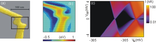
Figure 1. a) SEM micrograph of the gate structure (yellow) on the crystal surface (grey). The dashed rectangle marks the area used in (b) Numerically calculated conduction band deformation at the 2DES. The colour scale describes energy in eV. (c) Coulomb diamonds measured on a single gate quantum dot (after [1]).
Fig. 1 (c) displays the current through the 2DES across the gate as a function of bias voltage VSD and gate voltage VG (with respect to the 2DES). For sufficiently negative voltage VG the 2DES is separated in two halfs preventing current flow (left side of Fig. 1(c)). In the opposite regime of VG=0 current flows freely through the 2DES. However, in the intermediate voltage range we observe diamond shaped regions of low current (Fig. 1 (c)) marking Coulomb blockade typical for a quantum dot. The result of a numerical calculation using the simulation tool nextano3 [2] is plotted in Fig. 1 (b). This Schrödinger-Poisson solver takes the full crystal structure as well as mechanical stress and the piezoelectric effect present in GaAs into account. Tensional stress is caused by different thermal expansion coefficients of gold (top gate) and GaAs (wafer). The potential minimum at the right hand side to the center of the top gate explains well the existence of the observed single-gate quantum dot. Remaining minimas along the gate cannot form a quantum dot since they proceed along the whole gate without forming a pronounced minimum. Further experiments will investigate the tunability of such quantum dots and more complicated structures as a single gate double quantum dot.
- C. Rössler, Diploma thesis, Institute for Nano Physics, LMU München (2004)
- http://www.wsi.tum.de/nextnano3/index.htm
An on-chip quantum noise detector
Vadim Khrapay, Stefan Ludwig, and Jörg P. Kotthaus, in collaboration with Werner Wegscheider
Fluctuations of electric current or voltage contain additional information, not accessible via time-averaged quantities such as the dc-resistance, about the non-equilibrium properties of a mesoscopic system [1]. We have built an on-chip quantum detector close by a mesoscopic emitter of quantum fluctuations. Our detector possesses an extremely wide band width as well as a high sensitivity compared to classical noise detection schemes [2]. The nano structure is laterally defined by means of metal gates deposited in our clean room on the surface of a GaAs/AlGaAs heterostructure (Fig. 1). The central gate C is used to divide the two dimensional electron system (2DES) 90 nm below the wafer surface into emitter and detector circuits. If gate C is accordingly biased, no electric current can flow between them. Depending upon the voltages applied to gates 1-10 we can define combinations of quantum point contacts (QPC), quantum dots, or double quantum dots as emitter and detector.
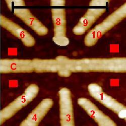
Figure 1. AFM micrograph of the laterally defined nanostructure. Metallic top gates are marked with numerals. Black squares mark the regions of the 2DES used for source and drain contacts. The black bar on the bottom corresponds to the length of one micrometer.
In Fig. 2 we present a measurement for the simplest case, where both the emitter and the detector are QPCs formed by biasing gates 3, 8, and C , respectively. The green dashed line represents the linear response conductance through the detector QPC, where the plateaus correspond to even multiple of the conductance quantum e2/h. After this QPC characterization we applied a relatively high bias voltage across the emitter QPC generating a current and then measured the current through the unbiased detector QPC. As expected, the detector current stays zero if the emitter QPC is tuned to be on one of its conductance plateaus. However, for the emitter QPC tuned halfway between zero conductance and its first plateau we observe a pronounced current through the detector which flows in the opposite direction as the emitter current (blue solid line). More detailed measurements including combinations of quantum dots and double quantum dots as detector or emitter suggest a noise induced drag effect as the origin of the detector current. Intriguingly, shot noise and classical Coulomb drag can not fully explain our observations.
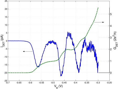
Figure 2. Detector current measured with a lock-in amplifier (emitter bias 2.1 mV) as a function of detector gate voltage (blue curve), for zero bias on the detector. Also shown is conductance of the detector QPC (green curve), numbers 0, 1, 2, 3 marking the plateaus quantized in units of e2/h.
- Ya. M. Blanter and M. Buettiker, Phys. Rep. 336, 1 (2000)
- R. Aguado and L. Kouwenhoven, Phys. Rev. Lett 84, 1986 (2000)
Freely Suspended Quantum Dots
Clemens Rössler, Stefan Ludwig, and Jörg P. Kotthaus, in collaboration with Max Bichler, Dieter Schuh, and Werner Wegscheider
We employ quantum dots embedded in nanoscale phonon cavities in order to investigate the electron-phonon interaction. Our phonon cavities are nanoscale bridges excavated from an AlGaAs/GaAs heterostructure. The latter contains a two-dimensional electron system (2DES) which is depleted locally by applying a negative voltage to metallic top gates (Fig. 1).
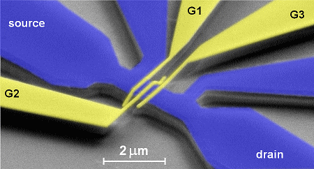
Figure 1. SEM micrograph of a freestanding structure taken under a tilt angle of 60 degrees. Three golden gates G1, G2, G3 lie on top of the underetched GaAs/AlGaAs heterostructure. Electrons flow from source to drain.
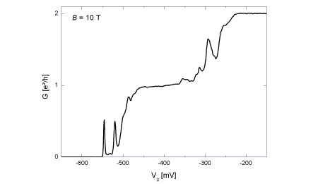
Figure 2. Differential conductance G of the freestanding bridge as a function of the voltage applied to gate G2 (see Fig. 1). The contact resistance R = 2,4 kOhm is subtracted in this two-terminal measurement.
Optics with nanostructures
The interaction between photons and semiconductor nano-structures is at the center point of our research. To this end, optically generated excitons are studied in various solid state systems. In order to extract the drift mobility of indirect excitons in coupled GaAs quantum wells, A. Gärtner et al. employ the quantum confined Stark effect in combination with a resistive top gate of a field-effect device to realize time-of-flight experiments for drifting excitons. By measuring the photoluminescence of recombining excitons as a function of space, energy, and time, the excitonic drift dynamics are resolved across several hundreds of microns. C. Dupraz et al. study the optoelectronic properties of single carbon nanotubes. In combination with a resonant optical excitation, single electron transport through carbon nanotubes provides insight into the optoelectronic characteristics of a system with dimensionally constrained densities of electrons and phonons. Generally, excitons in self-assembled quantum dots constitute an atomic-like solid state system ideally suited to study quantum properties, while it is attractive for realizing qubits. A. Högele et al. demonstrate how the electron-hole interaction in a single quantum dot can be controlled simply by applying a voltage to macroscopic gates. Key technology for such experiments is a high resolution laser absorption spectroscopy of single InGaAs/GaAs self-assembled quantum dots embedded in a field-effect structure. The technique is further exploited to manipulate the spin quantum number of single electrons via the Zeeman interaction in combination with a (Pauli) blockade.
Exciton dynamics in voltage-tunable mesoscopic landscapes
Andreas Gärtner, Alexander W. Holleitner, and Jörg P. Kotthaus, in collaboration with Dieter Schuh
Photo-generated electron-hole pairs in quantum well devices can be manipulated in lifetime and position via mesoscopic voltage-controlled electrostatic landscapes [1]. These devices attract much interest, because experiments aiming to observe Bose-Einstein condensation of excitons require a flexible control over the exciton dynamics [2]. Here we employ the quantum confined Stark effect in a coupled double GaAs/AlGaAs quantum well structure to generate spatially indirect excitons with lifetimes exceeding 100 ns [3]. To control the excitonic motion we impose voltage-tunable lateral potential gradients for long-living excitons by utilizing current-carrying resistive top gates as sketched in Fig. 1 [4]. We study the drift dynamics of the excitons in time-of-flight experiments by resolving the emitted photoluminescence in space, energy and time simultaneously. As shown in Fig. 2 we find high exciton mobilities exceeding 105 cm2/eVs at temperatures below 10 K [4]. Future excitonic traps based on this technique could be easily extended towards optoelectronic solid-state devices due to the potential scalability and compatibility with existing semiconductor technology.
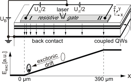
Figure 1. Experimental setup (upper image) to create a gradient potential for excitons (lower image). See text and ref. [4] for details.
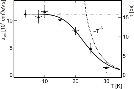
Figure 2. Excitonic mobility µ as a function of the temperature T. See ref. [4] for details.
- S. Zimmermann et. al., Phys. Rev. B 56, 13414 (1997).
- L. V. Butov et al., Nature 417, 47 (2002).
- A. Gärtner et al., Physica E 32, 195 (2006).
- A. Gärtner et al., Appl. Phys. Lett. 89, 052108 (2006).
Photo-induced Conductance in Carbon Nanotubes
Christian J.-F. Dupraz, Udo Beierlein, and Jörg P. Kotthaus
In recent years intense research has broadened the knowledge of the physical properties of carbon nanotubes. Here we combine optical spectroscopy and conductance measurements on single and multi wall carbon nanotubes in order to study their optoelectronic characteristics. Standard lithography techniques are used to contact carbon nanotubes. The carbon nanotubes are either contacted by evaporating metallic contacts onto their ends, or by positioning the carbon nanotubes on top of prefabricated metallic electrodes. By both techniques, two or four point geometries can be realized. Photoconductance measurements are carried out in the temperature range between 2 K and 300 K. The nanotubes are optically excited by a laser, while the photoconductance is measured by a lock-in-technique. A Fourier-spectrometer is exploited to gain the spectral information of the photo-induced conductance of the carbon nanotube for wavenumbers between 800 cm-1 and 12000 cm-1. Fig. 1 shows a typical measurement of the photocurrent of a single wall nanotube-device illuminated by a He-Ne-Laser at 4.2 K. The maximum photo-response is detected in the Coulomb blockade regime at low bias.
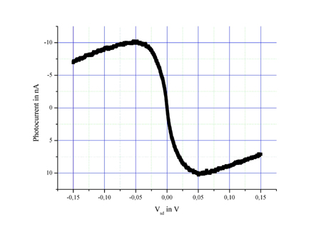
Figure 1.
A corresponding energy spectrum obtained by the Fourier-spectrometer is depicted in Fig. 2. We compare two spectra; one detected at 2 K with one at 8 K. Clearly, a peak at 6000 cm-1 can be seen, that can be assigned to a van-Hove singularity.
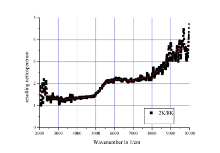
Figure 2.
Spin-selective optical absorption of singly charged excitons in a quantum dot
A. Högele, S. Seidl, M. Kroner, R. J. Warburton, and K. Karrai, in collaboration with M. Atatüre, J. Dreiser, A. Imamoglu, B. D. Gerardot, P. M. Petroff.
We report high resolution laser absorption spectroscopy of a single InGaAs/GaAs self-assembled quantum dot embedded in a field-effect structure. We show experimentally that the interband optical absorption to the lower Zeeman branch of the singly charged exciton is strongly inhibited due to spin (Pauli) blockade of the optical transition. At high magnetic fields the optical absorption to the upper Zeeman branch dominates the absorption spectrum. We find however that the spin blockade is not complete and a 10% leakage remains at high magnetic fields. Applying a gate voltage to empty the dot of its resident electron turns the spin blockade off. This effect is observed at 1.5 K and up to 9 Tesla [1].
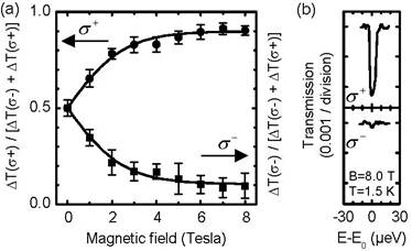
Figure 1. (a) Evolution of the relative resonance intensities with magnetic field for both circular polarizations. The solid lines are fits to the data with electron g-factor |ge|=1.8 and an empirical limit to the maximum achievable electron spin polarization of about 90% in order to account for the fact that the lower energy absorption branch does not vanish at high fields. The temperature was 1.5 K. (b) Differential transmission spectra of the right-hand circular (upper panel) and left-hand circular (lower panel) transition at a magnetic field of 8.0 T.
- A. Högele et al., Appl. Phys. Lett. 86, 221905 (2005)
Voltage-controlled electron-hole interaction in a single quantum dot
A. Högele, S. Seidl, M. Kroner, R. J. Warburton, and K. Karrai, in collaboration with M. Atatüre, J. Dreiser, A. Imamoglu, B. D. Gerardot, P. M. Petroff.
The ground state of neutral and negatively charged excitons confined to a single self-assembled InGaAs quantum dot is probed in a direct absorption experiment by high resolution laser spectroscopy. We show how the anisotropic electron-hole exchange interaction depends on the exciton charge and demonstrate how the interaction can be switched on and off with a small dc voltage. Furthermore, we report polarization sensitive analysis of the excitonic interband transition in a single quantum dot as a function of charge with and without magnetic field [1].
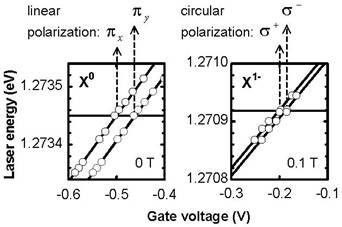
Figure 1. Voltage control of polarization in a single quantum dot. Resonance energies of linearly polarized X0 transitions at zero magnetic field (left) and circularly polarized X1- transitions at 0.1 Tesla (right) as function of gate voltage. The data were taken at 4.2 K.
- A. Högele et al., Journ. of Supercond. 18, 245 - 249 (2005).
Nanomechanical Systems
Nanomechanical systems are realized by lithographic techniques that are capable to create freestanding objects in silicon and other materials, with thickness and lateral dimensions down to about some 10 nanometers. Shrinking mechanical devices in thickness and width leads to reduced mass, increased resonant frequency, and lowered force constants of these systems. Therefore nanomechanical systems are both fascinating objects for fundamental studies in the quantum regime and promising for a large variety of applications such as extremely sensitive sensors and actuators. Advances in the field include improvements in fabrication processes, new methods for actuating and detecting motion at the nanoscale. A still challenging problem is how to easily excite nanomechanical elements and control their motion. In both areas we achieved substantial progress.
Highly Efficient Laser Driving Scheme for Bilayer Nanoelectromechanical Systems
Daniel R. König and Jörg P. Kotthaus
Nanoelectromechanical Systems (NEMS) are of increasing interest in fundamental research. As NEMS are continuously scaled down they are starting to approach the quantum limit [1]. Their applications range from highly sensitive detectors and fast switches to frequency filters and spin-detectors [2,3,4,5]. Dynamic NEMS operation requires reliable and efficient driving mechanisms. We developed a laser actuation mechanism which efficiency and reliability is competitive with the widely used magneto motive drive. We use a pulsed 5 mW diode laser with a wavelength of 633 nm to periodically heat a bi-layer beam resonator with its eigenfrequency. The resonators dimensions are 10 µm length, 200 nm width, and 200 nm height. The height is composed out of 100 nm silicon and 100 nm gold. Due to the thermally induced stress caused by the different thermal expansion coefficients of the two layers the resonator is periodically deflected. For detecting the mechanical response, the resonator is placed in a magnetic field of 12 Tesla at 4 Kelvin and the induced Lorentz current due to its mechanical motion is measured with a lock-in amplifier (Fig. 1). The resonator is easily driven into the non-linear regime. Amplitudes up to 140 nm are reached (Fig. 2). Even higher resonance modes with frequencies up to 36 MHz can be excited.
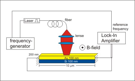
Figure 1. Laser actuation scheme: A pulsed 5 mW diode laser is focused onto a nano electromechanical beam resonator. Via the thermal induced mechanical stress the resonator is driven into resonance. The mechanical response is detected with a Lock-In-Amplifier by measuring the Lorentz current which is induced due to the magnetic field.
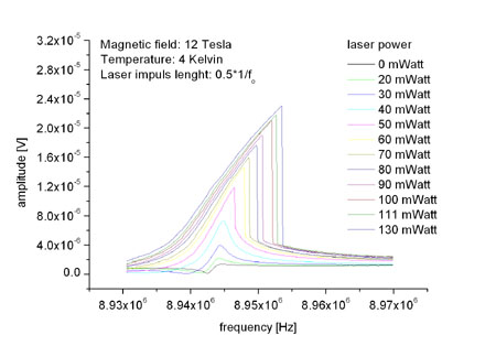
Figure 2. Resonance curves for different laser actuation powers. The beam resonator is driven into the non linear regime which is described by the Duffing-Equation.
- M. D. LaHaye, O. Buu, B. Camarota, and K. C. Schwab, Science 304,74 (2004)
- B. Ilic, Y. Yang, and H. G. Craighead, Appl. Phys. Lett. 85, 2604 (2004)
- J. E. Jang et al., Appl. Phys. Lett. 87, 163114 (2005)
- C. T.-C. Nguyen, IEEE Trans. Microwave Theory Tech. 47, 1486 (1999)
- D. Rugar, R. Budakian, H. J. Mamin, and B. W. Chui, Nature 430, 329 (2004)
Optical Imaging of Nanostructures
Alexander Ortlieb, Constanze Metzger , Christine Meyer, Ivan Favero, Heribert Lorenz, and Khaled Karrai, in collaboration with Omar Sqalli (attocube systems AG).
We have developed a slip-stick positioning system to work as a step-by-step scanning device [1]. Step sizes are ranging between 40 and 400 nm at room temperature and steps smaller than 5 nm are obtained at 4.2 K. Scanning confocal optical images on samples with nanomechanical systems are taken in reflectivity using a 635 nm wavelength laser and an objective of numerical aperture=0.8 (Fig. 1). They show exceptional low distortion and high linearity. The use of the slip-stick step motion for image scanning simplifies the scanning confocal microscope since the long-range positioning unit and the scanning unit merge into only one unit that can do both.
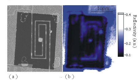
Figure 1. (a) SEM image of a completely free-standing Si3N4 nanostructure. (b) Optical image of the same structure by scanning confocal microscopy.
- C. Meyer, O. Sqalli, H. Lorenz, and K. Karrai, Rev. Sci. Instr. 76, 063706 (2005).
Nanobioscience
In the area of Nanobioscience, a variety of scientific questions at the boundary between nanoscience and biophysics were addressed. In one project, DNA molecules and the biochemical technique of rolling circle amplification were utilized for the realization of supramolecular assemblies which can serve as templates for the periodic arrangement of nanoparticles. In two other projects – which aim at the long-term realization of artificial molecular machines – nanomechanical DNA devices were controlled by i) genetic mechanisms and ii) by a chemical oscillator. The first approach was pursued in close collaboration with the group of Joachim Rädler. Finally, in cooperation with Nanion Technologies the nanofabrication facilities of the nanophysics group were utilized to build a biosensor based on a high-frequency coplanar waveguide which can detect the formation of a phospholipid bilayer and the incorporation of peptid pores therein.
DNA-templated assembly of nanoparticles
Stefan Beyer, Patrick Nickels, and Friedrich C. Simmel
Presently, the most sophisticated procedures for the self-assembly of nanoscale structures can be found in biochemistry. While in living systems, biochemical reaction networks are responsible for the organisation of biological complexity, simple biochemical reactions may also be "borrowed" to produce artificial structures. As an example, we utilized a well-established biochemical method – rolling circle amplification (RCA) – for the organization of colloidal gold nanoparticles into chains. In RCA, a DNA polymerase processively copies the sequence of a circular template strand, resulting in the generation of a long single-stranded product with a repeating sequence. This product can be hybridized to a complementary DNA strand bearing a specific chemical function, e.g. biotin. The resulting "chain of chemical functions" can then be utilized to spatially organize nanoscale particles.
- S. Beyer, P. Nickels and F.C. Simmel , Nano Letters, 5, 719-722 (2005).
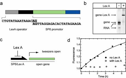
Genetic control of molecular devices
Wendy U. Dittmer, Susanne Kempter, Joachim O. Rädler, and Friedrich C. Simmel
DNA has been previously shown to be useful for the construction of nanomechanical devices such as DNA tweezers, a switchable protein-bearing DNA device based on an aptamer, or others [1]. As they are based on genetic material, DNA nanodevices quite trivially are compatible with gene regulatory mechanisms. This is extremely interesting if more complex and programmable self-assembly tasks are to be realized, as genetic circuits are known to perform a variety of computational tasks. In this way, the motion of DNA devices can be made dependent on environmental variables which are integrated in an information-processing genetic network. As one of the first steps in this direction we demonstrated how simple gene regulatory mechanisms based on the repressor proteins LacI and LexA can be used to control the opening or closing of DNA tweezers [2].
- F.C. Simmel and W.U. Dittmer , Small, 1, 284-299 (2005).
- W. U. Dittmer, S. Kempter, J.O. Rädler and F.C. Simmel , Small, 1, 709-712 (2005).
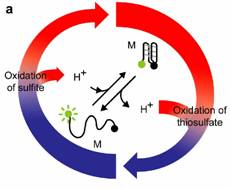
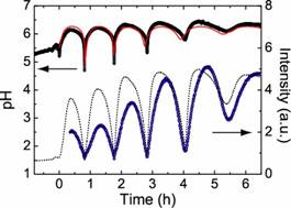
Driving nanodevices with chemical oscillators
Tim Liedl and Friedrich C. Simmel
Oscillating chemical reactions are fascinating nonlinear dynamical systems which have often been studied as "model systems" for biological rhythms and oscillations – even though these are usually considerably more complex. In our group, chemical oscillators are investigated as chemical "pace-makers" which may enforce temporal ordering in self-assembly and self-organization processes. As a very simple example, the conformational change of a cytosine-rich DNA sequence to a folded structure at low pH values (the so-called "i-motif") was coupled to pH oscillators generated by a relative of the well-known Landolt reaction. The pH oscillations continuously drive the DNA structures within a stirred semibatch tank reactor. After the reaction is started, the resulting DNA device system runs autonomously without any external intervention [1].
- T. Liedl and F.C. Simmel , Nano Lett, 5, 1894-1898 (2005).
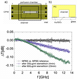
High-frequency detection of nanopore formation
Michael Olapinski, Stephan Manus, Michael George, Andrea Brüggemann, Niels Fertig and Friedrich C. Simmel
Cells communicate with their environment via membrane-bound proteins. Among the most important of these are ion channel proteins which carry transmembranal ionic currents and may switch conductance in response to environmental influences. Many ion channels are important drug targets and therefore are at the focus of pharmaceutical research efforts. Artificial lipid bilayers and pore-forming peptides are very simple model systems for cell membranes and ion channels. In this study (in collaboration with Nan]i[on Technologies), we investigated whether it is possible to detect the formation of peptide pores in a lipid bilayer supported on a microfabricated glass chip in transmission experiments at GHz frequencies. To this end, a coplanar waveguide was defined on the chip and integrated with a microfluidic cartridge. Lipid membranes were deposited on the waveguide using a vesicle fusion method. The deposition of the bilayers resulted in a significant change in the high frequency transmission properties of the waveguide. As an ion channel forming peptide, alamethicin was integrated into the bilayers. The influence of the pore forming peptides could also be clearly detected in the transmission signal. The transmission is expected to be mainly sensitive to dissipative effects associated with the buffer solution. The formation of pores in the bilayer varies the influence of these dissipative effects on the transmission.
- M. Olapinski, S. Manus, M. George, A. Bruggemann, N. Fertig, and F.C. Simmel , Applied Physics Letters, 88 (2006).
Diploma theses completed in 2005
- Tobias Smorodin
"Selbstorganisation von Kohlenstoff Nanoröhrchen durch chemische Funktionalisierung" - Hoi Nok Tsao
"Charge Transport in Pentacene Thin Film Transistors" - Eike Friedrichs
"Herstellung und Charakterisierung von RNA-Aptameren" - Sebastian Rèmi
"Laserspektroskopie an selbstorganisierten Halbleiterquantenpunkten" - Ulrich Hoyer
"Manipulation von Nanopartikeln auf chemisch modifizierten Oberflächen" - Matthias Fiebig
"Elektronische Transport-, Kapazitäts- und Photostrommessungen an Pentacen-Dünnschichttransistoren"
PhD theses completed in 2005
- Alexander Müller
"Sensorische Anwendungen mit akustischen Oberflächenwellen" - Christoph Strobl
"Mikro- und Nanofluidik auf piezoelektrischen Substraten" - Andreas Klaus Hüttel
"Gekoppelte Quantenpunkte im Bereich niedrigster Elektronenzahlen" - Alexander Högele
"Laserspektroskopie von einzelnen ladbaren Quantenpunkten"
Habilitations completed in 2005
- Friedrich C. Simmel
"Nanostrukturen und molekulare Maschinen aus DNA"
Guest scientists in 2005
- Professor Dr. Valeri Dolgopolov,
Russian Academy of Sciences, Chernogolovka, Russia, and Alexander von Humboldt Stiftung - Dr. Richard Warburton,
Heriot-Watt University, Edinburgh, United Kingdom, SFB 631 - Dr. Vadim Khrapay,
Russian Academy of Sciences, Chernogolovka, Russia, and Alexander von Humboldt Stiftung - Prof. Alexander O. Govorov,
Ohio University, USA, and Russian Academy of Sciences, Novosibirsk, and Alexander von Humboldt Stiftung - Dr. Carla Abilio,
Fundacào papa a Ciència e Tecnologia, Ministèry for Science and Technology, Portugal - Dr. Ivan Favero,
Ecole Normale Supèrieure, Paris Cedex, Frankreich, and Alexander von Humboldt Sitftung
Group members in 2005
Senior scientists
- Prof. Jörg P. Kotthaus
- Prof. Khled Karraï
- Dr. Udo Beierlein
- Dr. Alexander Holleitner
- Dr. Heribert orenz
- Dr. Stefan Ludwig
- Dr. Friedrich Simmel
- Dr. Eva Weig
Secretary
- Martina Jüttner
Technical staff
- Hans-Peter Kiermaier
- Wolfgang Kurpas
- Stephan Manus
- Alexander Paul
- Stefan Schöffberger
Ph.D. students
- Stefan Beyer
- Christian Dupraz
- Andreas Gärtner
- Alexander Högele
- Constanze Höhberger
- Klaus-Dieter Hof
- Andreas K. Hüttel
- Daniel König
- Martin Kroner
- Dawid Kupidura
- Tim Liedl
- Christine Meyer
- Michael Olapinski
- Andreas Reuter
- Clemens Rössler
- Dominik Scheible
- Daniel Schröer
- Bernd Zebli
Diploma students
- Stephan Camerer
- Matthias Fiebig
- Eike Friedrichs
- Ulrich Hoyer
- Alexander Ortlieb
- Sebastian Remi
- Nok Tsao
- Xaver Patrick Vögele
Publications in 2005
- T. Smorodin, U. Beierlein, and Jörg P. Kotthaus
"Contacting gold nanoparticles with carbon nanotubes by self-assembly"
Nanotechnology 16, 1123-1125 (2005) - Friedrich C. Simmel and Wendy U. Dittmer
"DNA Nanodevices"
Small 1, 284-299 (2005) - Stefan Beyer, Wendy U. Dittmer, and Friedrich C. Simmel
"Design Variations for an Aptamer-Based DNA Nanodevice"
J. Biomed. Nanotechnol.1, 96-101 (2005) - Stefan Beyer, Patrick Nickels, and Friedrich C. Simmel
"Periodic DNA Nanotemplates Synthesized by Rolling Circle Amplification"
Nano Lett. 5, 719-722 (2005) - Wendy U. Dittmer, Susanne Kempter, Joachim O. Rädler, and Friedrich C. Simmel
"Using Gene Regulation to Program DNA-Based Molecular Devices"
Small 1, 709-712 (2005) - Alexander Högele, Martin Kroner, Stefan Seidl, and
Khaled Karrai
Mete Atatüre, Jan Dreiser, and Atac Imamoglu
Richard J. Warburton, Antonio Badolato, Brian D. Gerardot, and Pierre M. Petroff
"Spin-selective optical absorption of singly charged excitons in a quantum dot"
Appl. Phys.Lett. 86, 221905-1 - -3 ( 2005) - M. Ediger, P. A. Dalgarno,J. M. Smith,
B. D. Gerardot,R. J. Warburton, K. Karrai,
and P. M. Petroff
"Controlled generation of neutral, negatively-charged and positively-charged excitons in the same single quantum dot"
Appl. Phys. Lett. 86, 211909-1 - -3 (2005) - J. M. Smith, P. A. Dalgarno, R. J. Warburton,
A. O. Govorov, K. Karrai, B. D. Gerardot,
and P. M. Petroff
"Voltage Control of the Spin Dynamics of an Exciton in a Semiconductor Quantum Dot"
Phys.Rev.Lett. 94, 197402-1 - -4 (2005) - Christine Meyer, Omar Sqalli, Heribert Lorenz
and Khaled Karrai
"Slip-stick step-scanner for scanning probe microscopy"
Rev. Sci. Instrum. 76, 063706-1 - -5 (2005) - A. Högele, S. Seidl, M. Kroner, K. Karrai,
R. J. Warburton, M. Atatüre, J. Dreiser, A. Imamoglu,
B. D. Gerardot, and P. M. Petroff
"Voltage Controlled Electron-Hole Interaction in a Single Quantum Dot"
J. Supercond. 18, 245-249 (2005) - Tim Liedl, Simon Keller, Friedrich C. Simmel,
Joachim O. Rädler, and Wolfgang J. Parak
"Fluorescent Nanocrystals as Colloidal Probes in Complex Fluids Measured by Fluorescence Correlation Spectroscopy"
Small 1, 997-1003 (2005) - R.J. Warburton, B. Urbaszek, E.J. McGheea, C. Schulhauser,
A. Högele, K. Karrai, B.D. Gerardot, and P.M. Petroff
"Charged magneto-exciton states in semiconductor quantum dots"
Physica E 26, 45-50 (2005) - Tim Liedl and Friedrich C. Simmel
"Switching the Conformation of a DNA Molecule with a Chemical Oscillator"
Nano Lett. 5, 1894-1898 (2005 ) - A. K. Hüttel, S. Ludwig, H. Lorenz,
K. Eberl, and J. P. Kotthaus
"Direct control of the tunnel splitting in a one-electron double quantum dot"
Phys. Rev. B 72, 081310-1 - -4 (2005) - Paul A. Dalgarno, Jason M. Smith, Brian D. Gerardot,
Alexander O. Govorov, Khaled Karrai, Pierre M. Petroff, and
Richard J. Warburton
"Dark exciton decay dynamics of a semiconductor quantum dot"
Phys. Status Solidi (a) 202, 2591–2597 (2005) - S. Seidl, M. Kroner, P. A. Dalgarno, A. Högele,
J. M. Smith, M. Ediger, B. D. Gerardot, J. M. Garcia,
P. M. Petroff, K. Karrai, and R. J. Warburton
"Absorption and photoluminescence spectroscopy on a single self-assemble charge-tunable quantum dot"
Phys. Rev. B 72 (2005) - Tobias Smorodin, Udo Beierlein,
Jens Ebbecke, and Achim Wixforth
"Surface-acoustic-wave-enhanced alignment of thiolated carbon nanotubes on gold electrodes"
Small 1, 1188-1190 (2005)
Invited talks in 2005
Alexander Holleitner
- "Spin relaxation in low-dimensional nanostructures"
Summer School on Nanoelectronics organized by DFG Research Center for Functional Nanostructures Karlsruhe (CFN), Bad Herrenalb, Germany September 01-04, 2005 - "Spin relaxation in InGaAs wires: Transition from 2D to 1D"
International Symposium on Structure and Dynamics on the Nanometer Scale, Phase coherent and ballistic transport & spin dependent properties, Duisburg November 10-13, 2005 - "Spin relaxation in InGaAs wires: Transition from 2D to 1D"
Seminar talk in the group of Professor J. Feldmann, Center for Nanoscience (CeNS), Munich November 28, 2005
Andreas Hüttel
- "Controlling the Tunnel Splitting in a One-electron Double Quantum Dot"
16 th International Conference „Electronic Properties of Two-Dimensional Systems“ EP2DS-16, Hyatt Regency Albuquerque, New Mexico, USA July 10-15, 2005
Khaled Karrai
- "Cavity cooling of micromechanical systems"
March Meeting of the American Physical Society, L.A. March 21-25, 2005 - "High resolution laser spectroscopy of single quantum dots"
Symposium: Optical spectroscopy of single quantum structures 69. Spring Meeting of the German Physical Society, Berlin March 04-09, 2005 - "How to cool micro-mechanical systems with laser light"
International Workshop on Nanophotonics and Nanobiotechnology, Koc University, Istanbul June 28- July 08, 2005 - "Optics of quantum dots"
International Workshop on Nanophotonics and Nanobiotechnology, Koc University, Istanbul June 28- July 08, 2005 - "Resonant Rayleigh Scattering spectroscopy of quantum dots"
MRS Fall 2005 meeting, MRS Symposium: Quantum confined semiconductor nanostructures: Fabrication, physical properties and applications. November 28 - December 02, 2005
Jörg P. Kotthaus
- "Some Quantum Phenomena in Nanoelectromechanical Systems"
69. Spring Meeting of the German Physical Society, Berlin March 04-09, 2005 and Int. Symposium "Nanoscience and -Technology" , Mauterndorf, Austria March 29–31, 2005 - "Nanoelectronics Joins with Biomolecules"
Int. Workshop "NanoBionics III – from Molecules to Applications" , Marburg, Germany April 04–08, 2005
Stefan Ludwig
- "Quanteneffekte einzelner Elektronen in künstlichen Nanostrukturen"
GMM-Workshop (VDE/VDI-Gesellschaft für Mikroelektronik, Mikro- und Feinwerktechnik) "Devices nach CMOS", Infineon Technology AG, Munich, July 16-17, 2005 - "Controlling Single Electron Transport through a Double Quantum Dot"
342nd Wilhelm and Else Heraeus Seminar: Science & Technology of Inorganic Nanowires, Bad Honnef, Germany, February 13–16, 2005
Constanze Metzger
- "Cavity cooling of micromechanical systems"
NanoForum Linz, Johannes Kepler Uni Linz, Austria May 26-27, 2005 - CeNS Winterschool workshop in Mauterndorf, Austria February 21-25, 2005
Stefan Schöffberger
- "Top-down nanofabrication"
II/V Plasma Technology Workshop Oxford Instruments , Zurich, Switzerland September 13-14, 2005
Friedrich Simmel
- "Nanodevices based on DNA aptamers"
Scanning Probe Microscopies and Organic Materials XIV, Munich September 2005 - "DNA-based molecular devices"
BIOMACH meeting "From Molecular Switches to Molecular Motors", Ascona September 2005 - "Control for DNA-based molecular machines"
MPI Terrestrial Microbiology Seminar series"Environmental, Cellular, and Molecular Microbiology"
September 2005
Senior scientists of cooperating groups
- Gerhard Abstreiter, Max Bichler
Walter Schottky Institut, TU München, Germany. - S. James Allen
University of California, Santa Barbara, USA. - Thomas Bein
CeNS, LMU Munich, Germany. - Robert Blick
University of Wisconsin-Madison, USA. - Alik Chaplik
Institute of Semiconductor Physics, Novosibirsk, Russia. - Valeri Dolgopolov
Russian Academy of Sciences, Chernogolovka, Russia. - Karl Eberl
Max-Planck-Institut für Festkörperforschung, Stuttgart, Germany. - Jochen Feldmann
CeNS, LMU München, Germany. - Jorge M. Garcia
Instituto de Microelectronica de Madrid, Spain. - Hermann Gaub, Wolfgang Parak
CeNS, LMU Munich, Germany. - Arthur C. Gossard
Materials Department, University of California - Santa Barbara, USA. - Alexander O. Govorov
Institute of Semiconductor Physics, Novosibirsk, Russia, and Ohio University, USA - Reinhard Guckenberger
MPI of Biochemistry, Martinsried, Germany. - Theodor W. Hänsch
LMU Munich, Germany. - Wolfgang Heckl
CeNS, LMU Munich, Germany. - Atac Imamoglu
Department of Physics, ETH Swiss Federal Institute of Technology, Zurich - Karl-Heinz Kunzelmann
Dental Science, LMU, Munich - Paul Leiderer
University of Konstanz, Germany. - Axel Lorke
Universität Duisburg-Essen, Germany. - Pierre M. Petroff
University of California - Santa Barbara, USA. - Joachim Rädler, Bert Nickel
LMU München, Germany. - Mansour Shayegan
Princeton University, USA. - Ulrich Schubert
Eindhoven University of Technology, Dutch Polymer Institute, Eindhoven, Netherlands - Richard Warburton
Heriot-Watt University, Edinburgh, U.K. - Werner Wegscheider, Christoph Strunk, Dieter Schuh
Institut für Angewandte und Experimentelle Physik, Universität Regensburg, Germany. - Andreas Wieck
Ruhr-Universität Bochum, Germany. - Achim Wixforth
Universität Augsburg, Germany.
Financial support in 2005
Funding of this work via the following agencies is gratefully acknowledged: