

Research report 1999
Preface
This is our 6th web-based research report since we went 'online' in 1994. Since then, our website has attracted a lot of attention from all over the world and meanwhile serves as an information source not only for our physics colleagues and interested students but also for those out there, who simply want to know on which subjects their 'tax Euros' are working. We appreciate the tremendous activity on our server and do encourage everybody to come by and stay for a while - also: Why don't you leave a note in our guestbook?
This year, however, we slightly changed the appaerance of our report: Instead of sub dividing our research activities into chapters we now cluster the activities into the different research groups as shown on our homepage. We hope that you can accustom to this new style.
Overview
Modern semiconductor technology nowadays combines more than ten million different transistors on a single chip barely as big as a thumbnail to form an extraordinary complex and sophisticated circuit. Following Moore's law, this very large scale integration will proceed over roughly the next ten years until a single element on a chip will be scaled down to less than about 50 nm. This typical dimension of a single device, however, represents a barrier, beyond which the basic operation of an electronic device starts to be based on fundamentally different mechanisms as compared to the conventional ones.
In a classical silicon MOSFET, for example, the principle of operation is based upon the statistical motion of about 10'000 electrons per square micron, whose number may be varied by an external electrode via electric fields. This movement takes place close to the relatively rough silicon/silicon dioxide interface and is described by diffusive processes, similar to the Brown's motion of molecules.
If, however, the dimension of a device becomes comparable or even smaller than the typical distance between two scattering events, the electrons start to move ballistically, like the balls on a billiard table. Moreover, at these small sizes, the number of electrons within a single device starts to approach one. For even smaller devices, their size becomes comparable to the wavelength of the electrons themselves - typically some ten nanometers in this case: The description of the electrons behaving like little charged spheres starts to fail and to require for a quantum mechanical formulation of the device.
In our group, we investigate the electronic, electrooptical, and electromechanical properties of specially tailored semiconductor structures with typical dimensions of the order or less than 100 nm. Recently, we also started to process and investigate mechanical systems like resonators and oscillators on the nanometer scale. Our goal is the detailed understanding of the new physical phenomena associated with a dramatic reduction of size, to explore new grounds for future device applications, and to be prepared for the day when nano-electronics will take over the role of micro-electronicsand micro or nano-mechanics will open new routes to the tiny ultra small universe!
- to boldly go where no person has ever gone before!
The research in our group is based on three fundamental prerequisites:
- Nanotechnology
- Sophisticated electronic and optical experimental techniques
- Quantum mechanical concepts and analysis
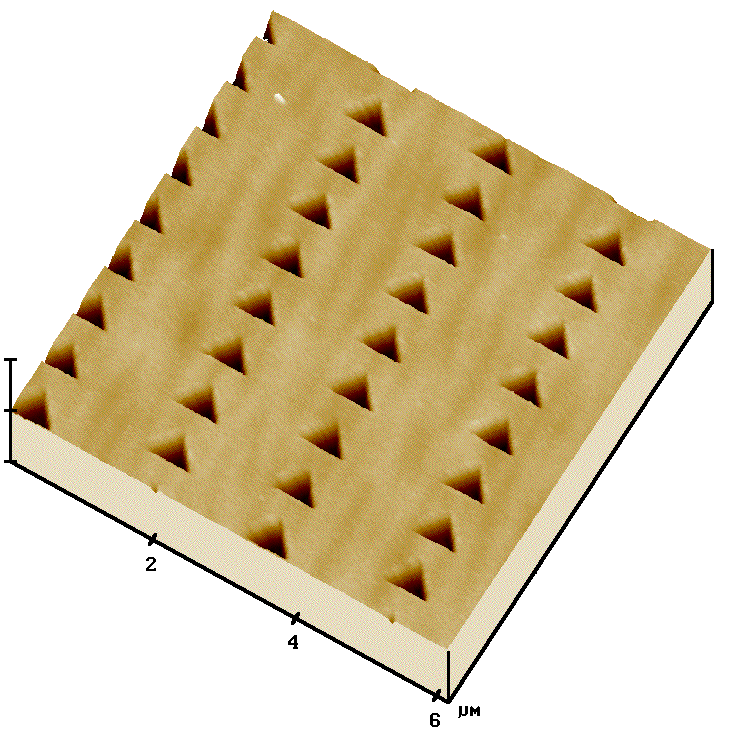
Starting from suited semiconductor layered systems, we first have to prepare the desired structures with lateral nanometer size dimensions. We use and develop different nanotechnologies that enable us to scale down the size of our structures to the size of the electronic wavelength. For this purpose, our nanotechnology labs are located in a dust free cleanroom area containing modern semiconductor processing equipment.
As we're always trying to be internationally competitive, we set up a large number of international co-operations with partners being specialized in the epitaxial growth of our high quality starting material. Meanwhile, our nanotechnological techniques are also transferred to different disciplines of leading edge research resulting in newly developed collaborations with highly qualified specialists in x-ray analysis, polymer physics and biophysics.
Secondly, we constantly develop and apply sensitive experimental techniques which enable us to chararcterize and to investigate the electronic and optical properties of our nanometer scale samples over the whole spectral range starting from DC over the microwave and infrared regime, the visible spectrum up to UV. At the same time, we are equipped with facilities allowing fo extremely low temperatures and high magnetic fields - invaluable tools for the detailed understanding of the quantum mechanic phenomena in our devices.
A third prerequisite for our research is a detailed and fundamental theoretical analysis and understanding of nanophysics. Together with many theoretical groups and in a very fruitful atmosphere of collaboration, we try to develop new theories and techniques helping us to understand or to predict the many fascinating effects that we are constantly facing. This is in particular important, as we are not studying systems already existing in nature but try to artificially tailor small pieces of this nature to behave in a desired fashion.
Summary of the different research topics
Prof. Dr. Jörg P. Kotthaus
Head of the group

Dr. Robert Blick
Nanomechanics, Quantum Dots, Ion Channels
Prof. Dr. Khaled Karraï
Near Field Optics
Scanning probe microscopy
Dr. Bert Lorenz
Silicon technology
STM / AFM
EBD materials

PD Dr. Achim Wixforth
Surface Acoustic Waves
FTIR Spectroscopy
Magnetotransport
PD Dr. Axel Lorke
Far Infrared Spectroscopy
Self assembled nonostructures
Semiconductor-cell hybrids
'99 Publications of the semiconductor group
- 1-99
M. Rotter, W. Ruile, A. Wixforth, and J. P. Kotthaus
"Voltage Controlled SAW Velocity in GaAs/LiNbO3-Hybrids"
IEEE Transaction on Ultrasonics, Ferroelectrics, and Frequency Control, Vol. 46, (1999) pp. 120-124.
- 2-99
I. Kegel, T. H. Metzger, P. Fratzl, J. Peisl, A. Lorke, J. M. Garcia, and P. M. Petroff "Interdependence of Strain and Shape in Self-Assembled Coherent InAs Islands on GaAs"
Europhys. Lett.45, 222-227 (1998).
- 3-99
Z. Kovats, T. Salditt, t. H. Metzger, J. Peisl, T. Stimpel, H. Lorenz, I. O. Chu, and K.Ismail "Interface Morphology in Strainerd Layer Epitaxy of Si/Si1-xGex Layers Studied by
X-Ray Scattering under Grazing Incidence and Atomic Force Microscopy"
J. Phys. D: Appl.Pys.32, 359-368 (1999).
- 4-99
S. Zimmermann, A. Wixforth, J. P. Kotthaus, W. Wegscheider, and M. Bichler
"A Semiconductor Based Photonic Memory Cell "
Science 283, 1292-1295 (1999).
- 5-99
M. Rotter, A. V. Kalameitsev, A. O. Govorov, W. Ruile, and a. Wixforth
"Charge Conveyance and Nonlinear Acoustoelectric Phenomena for Intense Surface Acoustic Waves on a Semiconductor Quantum Well"
Phys. Rev. Lett. 82, 2171-2174 (1999).
- 6-99
A. M. Song, S. Manus, M. Streibl, A. Lorke, J. P. Kotthaus, W. Wegscheider, and M. Bichler
"A Nonlinear Transport Device with no Intrinsic Threshold"
Superlattices and Microstructures 25, 269-272 (1999).
- 7-99
A. M. Song, A. Lorke, J. P. Kotthaus, W. Wegscheider, and M. Bichler
"Ballistic Magnetotransport in a Seminconductor Microjunction with Broken Symmetry" Superlattices and Microstructures 25, 149-152 (1999).
- 8-99
F. Simmel, David Abusch-Magder, D. A. Wharam, M. A. Kastner, and J. P. Kotthaus
"Statistics of the Coulomb-Blockade Peak Spacings of a Silicon Quantum Dot"
Phys. Rev. B 59, 10441-10444 (1999).
- 9-99
A. M. Song
"Formalism of Nonlinear Transport in Mesoscopic Conductors"
Phys. Rev. B 59,9806-9809 (1999).
- 10-99
R. J. Luyken. A. Lorke, M. Fricke, J. P. Kotthaus, G. Medeiros-Ribeiro, and P. M. Petroff "Coulomb-Coupling in Vertically Aligned Self-Assembled InAs Quantum Dots"
Nanotechnology 10, 14-17 (1999).
- 11-99
R. J. Luyken, A. Lorke, A. O. Govorov, and J. P. Kotthaus
"The Dynamics of Tunneling into Self-Assembled InAs Dots"
Appl. Phys. Lett. 74, 2486-2488 (1999).
- 12-99
R. J. Warburton, C. Bödefeld, C. S. Dürr, K. Karrai, J. P. Kotthaus, G. Medeiros-Ribeiro, and P. M. Petroff
"Charged Excitons in InAs Quantum Dots"
Festkörperprobleme/Advances in Solid State Physics 38, Ed. B. Kramer (Vieweg, Braunschweig/Wiesbaden 1999) pp. 180-192.
- 13-99
A. Wixforth
"Surfen im Nanokosmos"
Physik in unserer Zeit, 3/1999, p. 123-130.
- 14-99
V. T. Dolgopolov, A. A. Shashkin, E. V. Deviatov, F. Hastreiter, M. Hartung, A. Wixforth, K. L. Campman, and A. C. Gossard
"Electron Subbands in a Double Quantum Well at a Quantizing Magnetic Field"
Phys. Rev. B59, 13235-13241 (1999).
- 15-99
A. A. Shashkin, V. T. Dolgopolov, E. V. Deviatov, B. Irmer, A. G. C. Haubrich, J. P. Kotthaus, M. Bichler, and W. Wegscheider
"Lateral Tunneling through the Controlled Barrier between Edge Channels in a Two-Dimensional Electron System"
JETP Lett. 69, 603-609 (1999).
- 16-99
A. Lorke, R. J. Luyken, M. Fricke, J. P. Kotthaus, G. Medeiros-Ribeiro, J. M Garcia, and P. M. Petroff
"Electronic Structure of Nanometer-Size Quantum Dots and Quantum Rings"
Microelectronic Engineering 47, 95-99 (1999)
- 17-99
A. Wixforth, C. Rocke, S. Zimmermann, and J. P. Kotthaus
"Storage of Photonic Signals in Semiconductor Heterostructures"
Microelectronic Engineering 47, 317-319 (1999).
- 18-99
C. Obermüller, A. Deisenrieder, G. Abstreiter, K. Karrai, S. Grosse, S. Manus, J. Feldmann, H. Lipsanen, M. Sopanen, and J. Aholpelto
"Mechanical Nanomanipulation of Single Strain-Induced Semiconductor Quantum Dots"
Appl. Phys. Lett. 75, 358-360 (1999).
- 19-99
F. Simmel, R. H. Blick, J. P. Kotthaus, W. Wegscheider, and M. Bichler
"Anomalous Kondo-Effect in a Quantum Dot at Non-Zero Bias"
Phys. Rev. Lett. 83, 804-807 (1999).
- 20-99
A. O. Govorov, M. Rotter, M. Streibl, C. Rocke, A. V. Kalameitsev, A. Wixforth, and J. P. Kotthaus
"Acousto-Electric Transport through a Two-Dimensional System in the Nonlinear Regime"
Proc. of the 7th Int. Symposium "Nanostructures: Physics and Technology, St. Petersburg (Ioffe Institute 1999), pp-157-162.
- 21-99
T. Pompe, A. Frey. S. Herminghaus, A. Kriele, H. Lorenz, and J. P. Kotthaus
"Submicron Contact Printing Ion Silicon Using Stamp Pads"
Langmuir 15, 2398-2401 (1999)
- 22-99
A. Tilke, M. Vogel, F. Simmel, A. Kriele, R. H. Blick, H. Lorenz, D. A. Wharam, and J.. P. Kotthaus
"Low-Energy Electron Beam Lithography Using Calixarene"
J. Vac. Sci. Technol. B17 (4), 1594-1597 (1999).
- 23-99
H. Pettersson, R. J. Warburton, C. Bödefeld, J. P. Kotthaus, N. Carlsson, L. Landin, M.-E Pistol, W. Seifert, and L. Samuelson
"Excitons and Stored Charge in Self-Organized InAs Quantum Dots in InP"
Proc. 24 ICPS, Jerusalem 1998, #0531.PDF on CD-ROM (ISBN 981-02-4030-9), 1999.
- 24-99
S. de Haan, A. Lorke, J. P. Kotthaus, R. Hennig, M. Suhrke, W. Wegscheider, M. Bichler "Magnetotransport Properties of Arrays of Cross-Shaped Antidots"
Proc. 24 ICPS, Jerusalem 1998, #0531.PDF on CD-ROM (ISBN 981-02-4030-9), 1999.
- 25-99
V. T. Dolgopolov, A. A. Shashkin, E. V. Deviatov, F. Hastreiter, M. Hartung, A. Wixforth, K. L. Campman, and A. C. Gossard
" Magnetic-Field-Induced Hybridization of the Electron Subbands in a Coupled Double Quantum Well"
Proc. 24 ICPS, Jerusalem 1998, #0531.PDF on CD-ROM (ISBN 981-02-4030-9), 1999.
- 26-99
A. M. Song, A. Lorke, J. P. Kotthaus, W. Wegscheider, and M. Bichler
"Experimental and Theoretical Studies on Nonlinear Transport in Ballistic Rectifiers"
Proc. 24 ICPS, Jerusalem 1998. #0531.PDF on CD-ROM (ISBN 981-02-4030-9), 1999.
- 27-99
J. P. Kotthaus, A. O. Govorov, C. Rocke, A. Wixforth, S. Zimmermann, M. Bichler, G. Böhm, W. Wegscheider, and G. Weimann
"Optics of Carriers Trapped in Lateral Superlattices"
in "The Physics of Semiconductors", 24th ICPS Jerusalem 1998, Ed. D. Gershoni (World Scientific, Singapore, 1999), pp.113-120.
- 28-99
B. Irmer, F. Simmel, R. H. Blick, H. Lorenz, J. P. Kotthaus, M. Bichler, and W. Wegscheider "Nano-Ploughed Josephson Junctions as On-Chip Radiation Sources"
Superlattices and Microstructures 25,785-795 (1999).
- 29-99
M. C. Bödefeld, R. J. Warburton, K. Karrai, J. P. Kotthaus, G. Medeiros-Ribeiro, and P. M. Petroff
"Storage of Electrons and Holes in Self-Assembled InAs Quantum Dots"
Appl. Phys. Lett. 74, 1839-1841 (1999).
- 30-99
R. H. Blick, A. Erbe, A. Tilke, H. Krömmer, L. Pescini, S. Manus, A. Kriele, and J. P. Kotthaus "Nanomechanical Resonators Operating in the Radio Frequency Regime as Single
Charge Detectors" BLICK.PDF auf CD-ROM "Advances in Solid State Physics 39", Ed. Bernhard Kramer, (Vieweg, Braunschweig/Wiesbaden) 1999.
- 31-99
W. Sauer, M. Streibl, T. H. Metzger, A. G. H. Haubrich, S. Manus, A. Wixforth, and J. Peisl "X-Ray Imaging and Diffraction from Surface Phonons on GaAs"
Appl. Phys. Lett 75, 1709-1711 (1999).
- 32-99
S. de Haan, A. Lorke, R. Hennig, M. Suhrke, W. Wegscheider, and M. Bichler
"Magnetotransport Properties of Arrays of Cross-Shaped Antidots"
Phys. Rev. B 60, 8845-8848 (1999).
- 33-99
A. Wixforth
"Nanobeben auf dem Chip"
Einsichten 16, Universität München im Selbstverlag, 28-31 (1999)
- 34-99
W.J. Parak, M. George, H. E. Gaub, s. Böhm, A. Lorke
"The Field-Effect-Addressable Potentiometric Sensor/Stimulator (FAPS)- a New Concept for a Surface Potential Sensor and Stimulator with Spatial Resolution"
Sensors and Actuators B 58, 497-504 (1999).
- 35-99
A. Tilke, R. H. Blick, H. Lorenz, J. P. Kotthaus, and D. A. Wharam
"Coulomb Blockade in Quasi-Metallic Silicon-on-Insulator-Nanowires"
Appl. Phys. Lett. 75, 3704-3706 (1999).
- 36-99
M. Streibl, A. Wixforth, J. P. Kotthaus, A. O. Govorov, C. Kadow, A. C. Gossard
"Imaging of Acoustic Charge Transport in Semiconductor Heterostructures by Surface Acoustic Waves"
Appl. Phys. Lett. 75, 4139-4141 (1999).
- 37-99
Jörg P. Kotthaus
"Toward Efficient Smart Pixels"
Science 286, 2286-2287 (1999).
- 38-99
L. Pescini, A. Tilke, R. H. Blick, H. Lorenz, J. P. Kotthaus, W. Eberhardt, and
D. Kern
"Suspending Highly Doped Silicon-on-Insulator Wires for Applications in Nanomechanics"
Nanotechnology 10, 418-420 (1999).
- 39-99
A. Tilke, C. Rocke, and A. Wixforth
"Frequency- and Spin-Dependent Absorption of Surface-Acoustic-Waves by a 2D Electron Gas in the Quantum Hall Regime"
Physica E 5, 41-44 (1999).
Invited talks:
- Axel Lorke
"Electronic States and Excitations in Self-Organized InAs/GaAs
Nanostructures"
Low Energy Electrodynamics in Solids '99
Pecs/ Hungary, June 1999
- Axel Lorke
"Ballistic Rectification in Semiconductor Nano-Structures with Broken Symmetry."
Centennial Meeting of the American Physical Society
Atlanta/ USA, March 1999
- Heribert Lorenz
"Quanten-Dots: Möglichkeit zur Realisierung eines Quantenprozessors"
Workshop "Quanteninformatonsverarbeitung", Düsseldorf, 1999
- Bernd Irmer
"Nanolithographie: klein ist fein"
Workshop "Nanoforum", Linz, 1999
- Jörg P. Kotthaus
"Nanostructured Semiconductors as Sensors and Manipulators"
Workshop on "Hierarchic Structure Formation and Function of Organic-Inorganic Hybrid Systems" (Ulm, Germany,1999)
- Jörg P. Kotthaus
"Manipulating Charges in Nanostructured Semiconductors"
1st IUPAC Workshop on Advanced Materials: Nanostructured Systems (Hongkong, China 1999)
- Jörg P. Kotthaus
"Manipulating Electrons in Nanostructured Semiconductors"
XXVIII Int. School on Physics of Semiconducting Compounds
"Jaszowiec '99" ( Jaszowiec, Poland, 1999)
- Jörg P. Kotthaus
"Excitons in Static and Dynamic Lateral Superlattices as Photonic Memories"
Nato ARW "Optical Properties of Semiconductor Nanostructures"
( Jaszowiec, Poland 1999)
- Jörg P. Kotthaus
"Manipulating Excitons and Electron-Hole Pairs in Static and Dynamic Superlattices"
Winterschool on "Low-Dimensional (<2D) Electron Systems in Solids"
(Les Houches, France, 1999)
- Jörg P. Kotthaus
"Electronic Structure and Single Electron Charging in Self-Assembled Quantum Dots"
Winterschool on "Low-Dimensional (<2D) Electron Systems in Solids"
(Les Houches, France, 1999)
- Jörg P. Kotthaus
"Eigenschaften selbstgeordneter Quantendots"
DFG Rundgespräch " Aspekte nanoskaliger Systeme"
(Bad Honnef, Germany, 1999)
- Achim Wixforth
"Surface Acoustic Wave Nanostructures"
DARPA/MEMS workshop "Nanoelectromechanical Systems (NEMS),
San Diego, April 22/23, 1999
- Achim Wixforth
"Nano-Beben auf dem Chip"
Scientific Colloquium "Frontiers in Nanoscale Chemistry and
Biochemistry"
Forschungszentrum Karlsruhe, 7./8. Oktober 1999
- Robert Blick
"Nanomechanische Resonatoren"
Kolloquiumsvortrag,
Universität Hamburg, Oktober, (1999).
- Robert Blick
"Quantum Computation with laterally gated Quantum Dots"
Naval Research Laboratories, Conference on 'The Physics of Quantum Dots for Quantum Computing', Washington, USA, September (1999).
- Robert Blick
"Mechanical Nano-Resonators"
Konferenz über Electronic Properties of two-dimensional Systems (EP2DS), Ottawa, Kanada, August (1999).
- Robert Blick
"A mesoscopic tool to study quantum coherent transport"
Workshop 'Statistical and dynamical aspects of mesoscopic systems', Sitges, Barcelona, Juni (1999).
- Robert Blick
"Kicking electrons with nanomechanical resonators"
CeNS Workshop in der Venice Internatinal University, Venedig, Italien, April (1999). - Robert Blick
"Nanomechanical resonators operating in the radio frequency regime as single charge detectors"
Frühjahrstagung der Deutschen Physikalischen Gesellschaft, Münster, März (1999).
Diploma- and PhD theses of 1999
Diploma theses completed in 1999
- Hannes Vogelmann
"Hochanregungsexperimente an parabolischen Quantentöpfen"
- Christoph Jabs
"Intrasubband-Plasmonen in InAs-Quantentöpfen"
- Helmut Krömmer
"Nanomechanische Resonatoren auf der Grundlage von freitragenden Gold-Silizium-Strukturen"
- Laura Pescini
"Suspended Nanostructures in Silicon-On-Insulator
- Niels Fertig
" Nanostrukturierte Meßsonde für einzelne Ionenkanäle in Zellmembranen"
- Bernhard Stein
"Rasterkraftspektroskopie an Halbleiterheterostrukturen bei tiefen Temperaturen"
- Christian Sebald
"Elektron-Loch-Transport mit akustischen Oberflächenwellen in niedrigdimensionalen Systemen"
- Eva Höhberger
"Magnetotransport in lateralen Halbleiterübergittern unter Einfluß vom Symmetriebruch"
- Christian G. Schäflein
"Optische Spektroskopie an einzelnen InGaAs-Quantenringen"
- Alexander Holleitner
"Mikrowellenspektroskopie an Quantenpunkten"
- Robert Alexander Wildfeuer
"Separate Kontaktierung von Randkanälen im Quanten-Hall-Effekt"
- Florian Beil
"Entwicklung komplexer Wandlergeometrien für akustische Oberflächenwellen in optoelektronischen Anwendungen"
PhD theses completed in 1999
- Bernd Irmer
"Nano-Lithographje mit dem Rasterkraftmikroskop: mesoskopische Tunnelstrukturen und Josephson-Kontakte"
- Barbara Jager
"Lokale Ferninfrarot-Spektroskopie nanostrukturierter 2-dimensionaler Elektronengase"
- Markus Rotter
"Wechselwirkung zwischen Oberflächenwellen und zweidimensionalen Elektronensystemen in LiNbO3/GaAs-Schichtstrukturen"
- Johannes Luyken
"Elektronische Eigenschaften von verspannungsinduzierten InGaAs/AlGaAs-Halbleiter-Nanostrukturen"
- Friedrich Simmel
"Transporteigenschaften von Quantenpunkten"
Guests in 1999
Guest Scientists, Visitors, and their Sponsors
- Prof. Valeri Dolgopolov
Institute of Solid State Physics, Russian Academy of Sciences, Chernogolovka, Russia
January 1 - February 28
SFB 348
- Prof. Robert Grober
Yale University, New Haven USA
February 15 - March 30
SFB 348
- Prof. Alexander Chaplik
Institute of Semiconductor Physics, Siberian Division, Russian Academy of Sciences, Novosibirsk, Russia
March 1 - April 30
SFB 348
- Prof. Mansour Shayegan
Princeton University, USA
June 1 - August 31
Alexander von Humboldt-Stiftung
- Prof. James S. Allen
University of California Santa Barbara, USA
July 1 - August 31
Alexander von Humboldt-Stiftung
- Hua Qin
Nanjing University, China
January 1 - December 31
VW-Stiftung / DAAD
- Prof. Alexander V. Govorov
Institute of Semiconductor Physics, Siberian Division, Russian Academy of Sciences, Novosibirsk, Russia
October 1 - December 31
Supplementary Lectureship
Financial Support:
Funding of this work via the following agencies is gratefully acknowledged:
- Deutsche Forschungsgemeinschaft
- Volkswagen-Stiftung
- Bundesministerium für Bildung und Wissenschaft, Forschung und Technologie (BMBF)
- Bayerische Forschungsstiftung FOROPTO
- Alexander von Humboldt - Stiftung
- European Community Project ESPRIT and TMR
- German - Israeli - Foundation
- Siemens AG München