

Bert Lorenz' research group
Fabrication and characterization of semiconductor nanostructures by atomic force microscopy
In collaboration with A. A. Shashkin, V. T. Dolgopolov and E. V. Deviatov at the Institute of Solod State Physics of the Russian Academy of Sciences in Chernogolovka we made a study on lateral tunneling between edge channels. At the depletion induced edges of a gated two-dimensional electron system, a gate-voltage controllable barrier arises when the donor layer of the heterostructure is partly removed along a fine strip by means of AFM lithography (link zu Paper 99-15). For a sufficiently high barrier the typical current-voltage characteristics is found to be strongly asymmetric, having a negative branch that corresponds to the current overflowing the barrier.
It is established that the barrier height depends linearly on both the gate voltage and the magnetic field, and the data are described in terms of electron tunneling between the outermost edge channels.

Figure 1. Top view of the tunneling device with the constriction after etching the AFM-oxidized part of the mesa structure.
Furthermore we optimized a new technique which enables the fabrication of highly transparent Josephson junctions in combination with mesoscopic devices as on-chip radiation sources (link zu Paper 99-28). We utilize a modified AFM tip to plough grooves into superconducting material, thus defining a weak link. This weak link is made within the superconducting split-gates, which are used to electrostatically form a conventional quantum dot and serves as a source of millimeter wave radiation around 100 GHz. We find that the millimeter wave emission of the weak link leads to a bolometric effect in the case of quantum point contact.

Figure 2. Nano-ploughed lines in an Al film. Left: a typical Dayem-style microbridge with dimensions L x W = 100 nm x 100 nm. Right: the loading force is increased from top to bottom, defining variable thickness bridges and bridges of increasing length L. The junction width W is easily adjusted by a horizontal displacement W, where the plough is withdrawn from the film.
X-ray investigations of strained Si/SiGe layers
In collaboration with Z. Kovats, T.H. Metzger und J. Peisl at the University of Munich the interface morphology in strained Si/SiGe epitaxial layers were studied by x-ray scattering and atomic force microscopy (AFM) (link zu Paper 99-3). The strain state of the layers was determined by grazing incidence diffraction (GID). Diffusive x-ray scattering under grazing incidence and exit close to the forwards direction revealed conformal roughness of the interfaces at lateral correlation lengths of about 1 micrometer. Surfaces have been investigated by AFM and exhibit anisotropies of RMS roughness and lateral correlation length along the (110) and (100) directions, which are parallel and diagonal to the cross-hatch pattern, respectively.
Submicron Silicon gratings for contact printing
For a collaboration with T. Pompe, A. Fery and S. Herminghaus at the Max-Planck-Institute of Colloids and Interfaces in Berlin (http://www.mpikg-golm.mpg.de/index_e.html) we fabricated surface gratings on silicon with typical periods ranging from 400 nm to 1000 nm and grooves with about 250 nm using holographic lithography followed by a dry etching process. These silicon nanostructures are used as masters to prepare silicon rubber stamps (link zu Paper 99-21), which are found to peel off the master easily even at wedge angles of 80 degrees if the master is silanized before. Stripe structures with periodicities down to 200 nm are feasible.
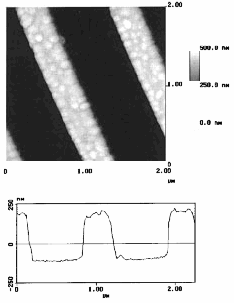
Figure 3. AFM topography image (top) of a typical silicon master grating. In the section cut perpendicular to the parallel grooves (bottom), the sharp and steep (incline angle is 80°) structure of the wall is clearly visible.
Electron beam lithography
We have used calixarene as a negative electron resist in combination with low-energy electron-beam lithography and investigated in the energy range between 0.5 and 20 keV (link zu Paper 99-22) for high resolution pattern definition.The suitability of electron energies down to 2 keV with a writing resolution of about 10 nm was clearly demonstrated. At low electron energies the required electron dose is drastically reduced. Moreover, irradiation damage during the exposure of a high-mobility two-dimensional electron gas using calixarene plays no significant role in the low-energy regime.
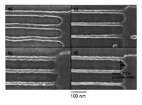
Figure 4. SEM picture of the test structure used for electron energies of 1, 2, 7, and 20 keV, respectively. Only a small influence of proximity effects can be seen at an electron energy of 20 keV, where the spatial range of the proximity induced line broadening is about 40 nm. At 1 keV (a) weak adhesion leads to curved lines. Using the obove metioned high-resolution low-energy electron-beam lithography and the negative electron resist calixarene, we succeeded in preparing silicon wires on highly doped silicon-on-insulator (SOI) films with a lateral extension of about 15 nm by reactive-ion-beam etching with CF 4 (link zu Paper 99-35). We demonstrated metallic Coulomb blockade in these silicon nanowires at temperatures up to almost 100 K.
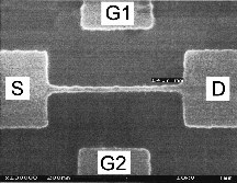
Figure 5. Scanning electron-beam micrograph of an etched, but not yet oxidized, and gated silicon quantum wire. The lateral dimensions can be scaled down to about 15 nm.
Furhermore we developed on a new method to build suspended silicon nanowires in highly doped silicon films in silicon-on-insulator substrates (link zu Paper 99-38). The beams are defined by high-resolution, low-energy electron-beam lithography using a two-layer positive electron resist. Micromachining techniques including dry and wet etching are applied to pattern the structures. We show first low-temperature measurements of these novel devices indicating electron-phonon interaction.
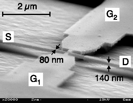
Figure 6. SEM micrograph of a suspended silicon quantum wire in a highly n-doped SOI film. As the n-silicon etches slowly during the underetching in HF, the starting film thickness of 190 nm is reduced to about 140 nm. The wire width is 80 nm and the length 1.5 µm. The suspended lateral side gates were not biased in the current experiments.
Literature
- 99-3
Z. Kovats, T. Salditt, t. H. Metzger, J. Peisl, T. Stimpel, H. Lorenz, I. O. Chu, and K.Ismail
"Interface Morphology in Strainerd Layer Epitaxy of Si/Si1-xGex Layers Studied by X-Ray Scattering under Grazing Incidence and Atomic Force Microscopy"
J. Phys. D: Appl.Pys.32, 359 - 368 (1999).
- 99-15
A. A. Shashkin, V. T. Dolgopolov, E. V. Deviatov, B. Irmer, A. G. C. Haubrich, J. P. Kotthaus, M. Bichler, and W. Wegscheider
"Lateral Tunneling through the Controlled Barrier between Edge Channels in a Two-Dimensional Electron System"
JETP Lett. 69, 603-609 (1999).
- 99-21
T. Pompe, A. Fery, S. Herminghaus, A. Kriele, H. Lorenz, and J. P. Kotthaus
"Performance of sub-micron contact printing on Silicon"
Langmuir 15, 2398 - 2401 (1999).
- 99-22
A. Tilke, M. Vogel, F. Simmel, A. Kriele, R. H. Blick, H. Lorenz, and J. P. Kotthaus
"Low-energy electron-beam lithography using calixarene"
J. Vac. Sci. Technol. B 17, 1594 - 1597 (1998).
- 99-28
B. Irmer, F. Simmel, R. H. Blick, H. Lorenz, J. P. Kotthaus, M. Bichler,
and W. Wegscheider
"Nano-Ploughed Josephson Junctions as On-Chip Radiation Sources"
Superlattices and Microstructures 25, 785-795 (1999).
- 99-35
A. Tilke, R. H. Blick, H. Lorenz, and J. P. Kotthaus, and D. A. Wharam
"Coulomb blockade in quasimetallic silicon-on-insulator nanowires"
Appl. Phys. Lett. 75, 3704 - 3706 (1999).
- 99-38
L. Pescini, A. Tilke, R. H. Blick, H. Lorenz, and J. P. Kotthaus,
W. Eberhard and D. Kern
"Suspending highly doped silicon-on-insulator wires for applications in nanomechanics"
Nanotechnology 10, 418 - 420 (1999).
Invited Talks
- H. Lorenz
"Quanten-Dots: Möglichkeit zur Realiisierung eines Quantenprozessors"
Workshop "Quanteninformatonsverarbeitung", Düsseldorf, 1999
- B. Irmer
"Nanolithographie: klein ist fein"
Workshop "Nanoforum", Linz, 1999
Doctoral Theses completed in 1999
- Bernd Irmer
"Nanolithographie mit dem Rasterkraftmikroskop: Mesoskopische Tunnelstrukturen und Josephson-Kontakte"
Financial Support
Funding of this work via the following agencies is gratefully acknowledged
- Volkswagen-Stiftung
- Bundesministerium für Bildung und Wissenschaft, Forschung und Technologie (BMBF)