

Research report 2010
- Introduction
- Electronic properties
- Optical and optoelectronical phenomena in nanodevices
- Electrostatically trapping indirect excitons in coupled InGaAs quantum wells
- Long exciton spin relaxation in coupled quantum wells
- Forming and confining of dipolar excitons by quantizing magnetic fields
- Photoluminescence of individual carbon nanotubes in static electric fields
- Imaging techniques for carbon nanotubes
- Nanomechanical systems
- Bachelor theses in 2010
- Diploma theses in 2010
- PhD theses in 2010
- Guest scientists in 2010
- Group members in 2010
- Publications in 2010
- Invited talks in 2010
- Senior scientists of cooperating groups
- Financial support in 2010
Introduction
Our research is focused on chip-based nanoscale devices and systems aiming at both, a deeper fundamental understanding of their physical behavior in the nanometer regime and the realization of novel devices, functions, and systems utilizing a broad spectrum of nanotechnologies.
Stefan Ludwig continues to successfully lead our research on nanoelectronic quantum transport, in part embedded in the DFG-funded SFB 631 “Solid-State Based Quantum Information Processing” and “Nanosystems Initiative Munich” (NIM). He also received a new DFG grant for his research on “Interactions between Mesoscopic Structures in Non-Equilibrium” and was granted a Heisenberg fellowship for 3 years starting 2012. Optical quantum control of GaAs-based quantum dots and carbon nanotubes is the major research focus of the nano-photonics group lead by Alexander Högele. Beyond his research efforts supported by the SFB 631 and NIM Alex has successfully started three new collaborative projects, one with Efrat Lifshitz (Technion, Haifa) funded by the German-Israeli-Foundation on “Magneto-Optical investigation of Multiple Excitons in Blinking-Free Colloidal Quantum Dots”, one with Stefan Ludwig and Jan von Delft seed-funded by NIM on “Optical Probes of Spin-Dependent Transport in Nanostructures: the 0.7 Anomaly” and another one with Tim Liedl funded by the Volkswagen Foundation on “Transfer of Energy and Information in DNA-Assembled Nanocrystal Networks”. His nano-optics research is complemented by our continuing DFG-funded optical studies on ensembles of spatially indirect, dipolar excitons generated in double quantum wells and fully confined via electrostatic traps. There we explore control of excitonic many-body interactions and possible phase transitions such as Bose-Einstein condensation. Our research on Nano-Electro-Mechanical Systems (NEMS), lead by Eva Weig and myself is still expanding, in part supported by the ongoing collaborative European project “Quantum Nano-Electro-Mechanical Systems” (QNEMS) coordinated by TU Delft and a DFG-funded project on “Nanoelectromechanical Resonators”. In addition Eva started a joint project with Doris Heinrich on “Dynamic Force Field Mapping of Living Cells in a Macro-Scale Transducer Array based on Flexible Semiconductor Nanopillars” generously supported by the Volkswagen Foundation.
In our research we profit from fruitful collaborations with quite a few colleagues within the “Nanosystems Initiative Munich” (NIM) and the Center for NanoScience (CeNS) as listed below as well as former members of our group, in particular Alexander Holleitner, now at TU Munich, Khaled Karrai at attocube and also honorary professor at LMU, and Sasha Govorov at Ohio University in Athens, USA. Stimulating interactions also result from extended stays of former and present Humboldt awardees and postdoctoral fellows, such as Valeri Dolgopolov of the Russian Academy of Sciences in Chernogolovka, Mansour Shayegan, Princeton University, Katarzyna Kowalik from the Grenoble High Field Laboratory, Eric Hoffmann from the University of Oregon, and Ivan Favero, now at Université Paris Diderot. Being embedded in both national and international collaborations further strengthens our research spectrum.
With the completion of 4 doctoral theses, 7 diploma theses, and 2 bachelor theses projects our educational efforts continue to be very successful. Similarly the 18 publications that were published in 2010 in renowned international journals and the numerous invited talks of members of our group at international conferences and workshops reflect well the breadth and depth of our research efforts. As additional acknowledgement Thomas Faust received the attocube-Wittenstein research award 2010 for his diploma thesis and a CeNS publication award 2010 was granted for our collaborative publication in Nano Letters. Fortunately, all members who left our group after completing their research projects were able to obtain attractive positions with good career perspectives.
As in previous years it is my special pleasure to thank all members of our group for their continued enthusiasm and excellent research effort. For those who have left us in 2010 I wish good luck on their new career track. Last but not least, I gratefully acknowledge the continuous generous support of our research by both national and international funding agencies. We hope that many readers worldwide enjoy this report and we are happy to receive any feedback.
Munich, May 5, 2011
Jörg P. Kotthaus
Electronic properties
Reducing the length scales of transistors well below 100 nanometers is one of the present key efforts in semiconductor industry. At the same time such tiny structures allow the observation of phenomena obeying the fundamental laws of quantum mechanics. In our clean room we fabricate a variety of gate-controlled devices by e-beam lithography starting from GaAs/AlGaAs heterostructures that contain a two-dimensional electron system (2DES). The gates lying on the sample surface can be voltage biased in order to locally deplete the 2DES. This technique allows us to further structure the 2DES and for instance create tunnel coupled zero-dimensional quantum dots or artificial molecules. The highlights in 2010 comprised a number of experiments on interactions in nonequilibrium nanoscale systems, ranging from phonon-mediated backaction via breakdown of the quantum Hall effect to avalanche amplification by electron-electron scattering. All these experiments are related to our efforts towards quantum computing, although this connection is even clearer for our experiments on the spin dynamics of electrons confined in double quantum dots. Here we perform measurements on GaAs/AlGaAs heterostructures, a mature material system, as well as on Si/SiGe based devices. Silicon promises longer spin-coherence times, because of the possibility to get rid of nuclear spins. In another experiment we developed a radio-frequency pulsed-gate spectroscopy technique and used it to measure tunnel splittings and energy relaxation times in a double quantum dot - a first step towards charge coherent measurements in coupled quantum dot systems. Our projects in 2010 relied on close collaborations with Gerhard Abstreiter (TU-München), Dominique Bougeard (University of Regensburg), Stefan Kehrein (LMU-München), Andy Sachrajda (NRC Canada), and Werner Wegscheider (ETH Zürich). Following we highlight few of our experiments:
Electron-avalanche amplifier based on the electronic Venturi effect
Daniela Taubert, Georg J. Schinner and Stefan Ludwig,
in collaboration with Hans-Peter Tranitz, Werner Wegscheider, Constantin Tomaras and Stefan Kehrein
Ballistic transport of electrons far from equilibrium is investigated in a cold
two-dimensional electron system. We observe scattering of excited charge carriers with the degenerate Fermi sea in a three-terminal device [1,2].
Amplification of the injected electron current can be achieved by energetically separating the electrons excited from the Fermi sea
from the conduction band holes they leave behind by means of a barrier, if additional electrons to neutralize the holes are supplied from a side contact.
The observed amplification effect depends on the energy of the injected electrons,
the injected current, and the height of the barrier used for separating
electrons and holes. A preliminary model based on numerical calculations using a random phase approximation is in agreement with our data.
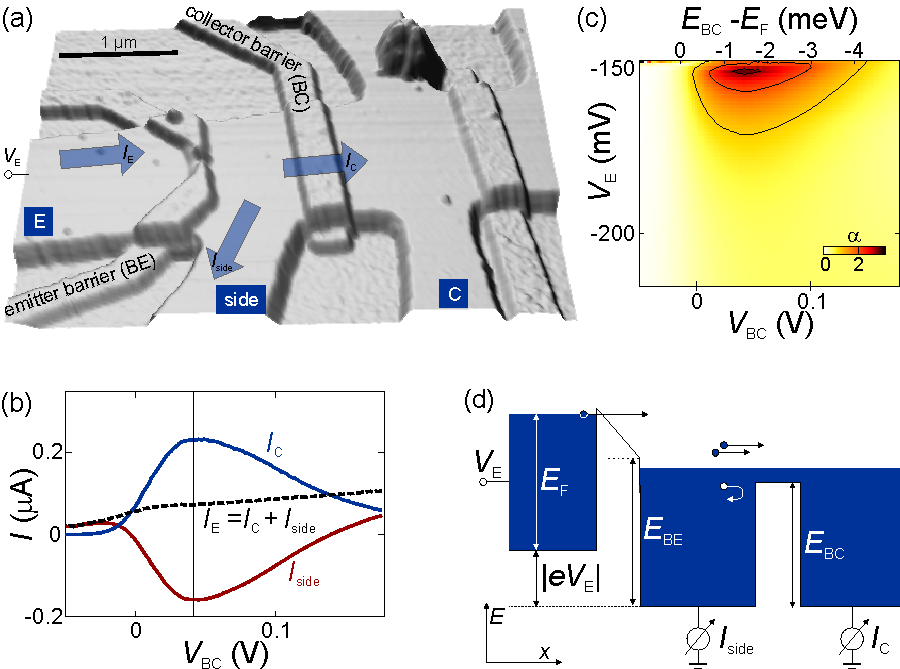
Figure (a) Atomic force micrograph of the sample. The elevated area contains a two-dimensional electron system. Gates fabricated on top of the sample are
used to define electrostatic barriers BE and BC. Ohmic contacts “E”, “side”, and “C”
are marked. (b) Currents measured at the contacts “side” and “C” as well as the total current IE as a function of the barrier voltage VBC.
Amplification is visible in the area with IC > IE, equivalent to Iside < 0. (c) Current amplification ratio α = iC / iE, plotted against barrier voltage VBC and bias VE, at the position marked in (b) by a vertical line. Contour lines show α = 1,2,3. (d) Energy diagram sketching the experiment.
- D. Taubert, G. J. Schinner, H. P. Tranitz, W. Wegscheider, C. Tomaras, S. Kehrein, and S. Ludwig, PRB 82, 161416R (2010)
- D. Taubert, G. J. Schinner, C. Tomaras, H. P. Tranitz, W. Wegscheider, and S. Ludwig, arXiv:1011.2289 (2010)
Spin dynamics in laterally defined few-electron double quantum dots with nanomagnet
Gunnar Petersen, Eric A. Hoffmann, Jörg P. Kotthaus and Stefan Ludwig,
in collaboration with Werner Wegscheider
It has been demonstrated that laterally defined double quantum dots in GaAs/AlGaAs heterostructures can be used as qubits. For instance a spin qubit has been realized in one of the two quantum dots as a single electron state split by an external homogeneous magnetic field. Our approach uses a monodomain nanomagnet to produce an inhomogeneous magnetic field up to 50 mT across a double quantum dot (see Figure 1). We plan to use this inhomogeneous field for all-electrical single electron spin resonance (ESR) measurements by applying an rf voltage to the gate beneath the nanomagnet. As a result, the electron confined in the quantum dot nearest the nanomagnet will oscillate in space and thereby experience an effective rf magnetic field. This allows manipulation of the spin qubit state while the second quantum dot is needed for initialization and readout of the spin qubit. In order to measure this manipulation, the double quantum dot is placed in Pauli spin blockade (see sketch in Figure 2). Figure 2 depicts current through the double quantum dot for positive (2a) and negative (2b) source-drain voltage as the quantum dot energy levels are swept by two gate voltages. In Figure 2a, current flows within the so-called bias triangle, while in Figure 2b, part of the current is absent due to Pauli spin blockade. Figure 3 shows the current through the spin-blockaded double quantum dot as a function of external magnetic field (parallel to the nanomagnet) and asymmetry energy (see arrow in Figure 2b).This current is caused by hyperfine interaction among the electron spin and many nuclear spins in the GaAs host material. This interaction allows spin-blocked triplet states to evolve into singlet states, thereby, lifting the spin blockade. Figure 3 demonstrates that this phenomena is most predominant at small asymmetry and small external magnetic field. In addition the fluctuations of the current at zero asymmetry can be attributed to dynamic nuclear spin polarization.
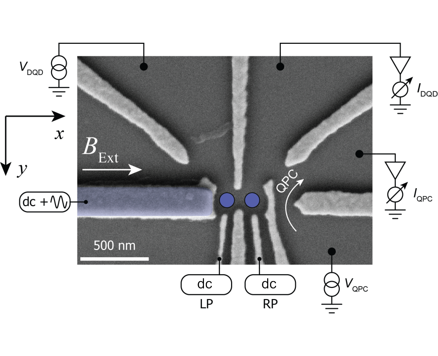
Figure 1. Scanning Electron micrograph of the sample surface. A double quantum dot and nearby quantum point contacts are defined by Ti/Au gates. A 50 nm thick monodomain cobalt nanomagnet is deposited on top of the left gate (gray-blue).
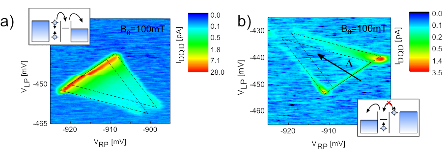
Figure 2. Current measurement of the biased double quantum dot. (a) For positive bias (0.8 mV) a small current is measured within the bias triangles.(b) For negative bias (-0.8 mV) current is blocked due to Pauli spin blockade (sketched in the insets).
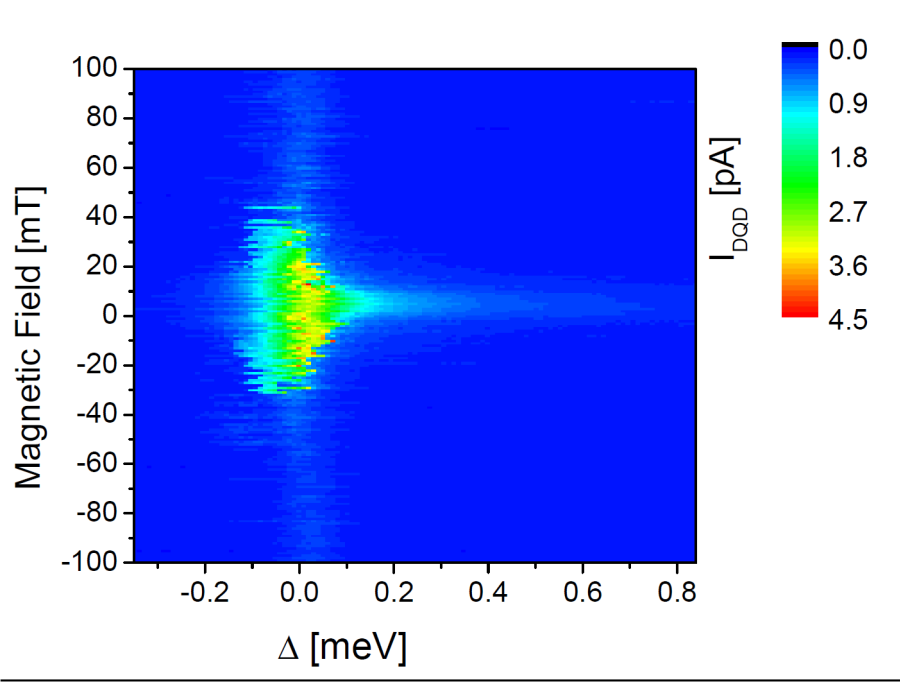
Figure 3. Measurement of the hyperfine interaction induced current through the double quantum dot for various magnetic fields as a function of the asymmetry Δ (along the arrow in figure 2b; Δ = 0 at the base of the triangle at finite current).
Pulsed gate charge spectroscopy on a Si/SiGe based double quantum dot
Andreas Wild, Jürgen Sailer, Joachim Nützel, Gerhard Abstreiter, Dominique Bougeard and Stefan Ludwig
In this project we transfer the so far GaAs based technology of laterally defined qubits to another material system, namely strained Si/SiGe heterostructures [1]. One of the advantages of silicon and germanium is the possibility to get rid of all nuclear spins by using isotope engineered materials. SiGe based spin qubits therefore promise much longer coherence times compared to GaAs based devices. We have already performed charge spectroscopy on a few-electron Si/SiGe double QD using a remote single QD sensor [2]. The heterostructure and gate layout of the double quantum dot are presented in Figure 1. The large effective electron mass (compared to GaAs) in this material causes low tunneling rates while it enhances their dependence on gate voltages. This property could be utilized for a very efficient pulsed gate control of the tunnel splitting, a component of several proposals for quantum information processing. The dependence of the interdot tunneling rate on the voltage applied to a control gate is shown in Figure 2, while Figure 3 shows a stability diagram demonstrating pulsed gate spectroscopy.
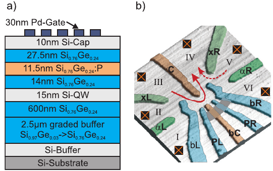
Figure 1. (a) Layout of the MBE Si/SiGe heterostructure showing the layer structure. Evaporated palladium gates deplete parts of the 2D electron gas in the silicon quantum well (Si-QW). (b) AFM micrograph of the gates defining the double QD. In addition, a single QD, defined by gates bR and xR, can be used as a charge sensor.
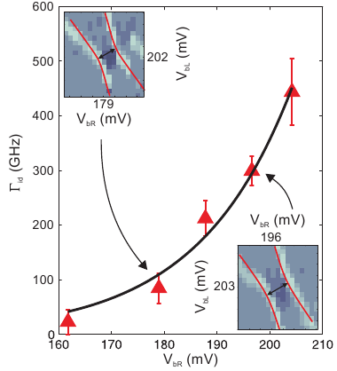
Figure 2. Inter-dot tunneling rate as a function of a control gate voltage. Insets show exemplary avoided crossings in the stability diagram. The solid line in the main plot is obtained via the Wentzel-Kramers-Brillouin (WKB) approximation.
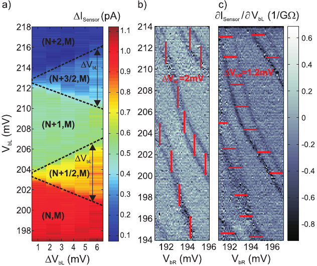
Figure 3. (a) Charge sensor current ISensor as a function of a control gate voltage which is modulated by a rectangular pulse sequence with 50% duty cycle. In between the charge plateaus where the two quantum dots are occupied by an integer number of electrons, i.g. (N,M), intermediate plateaus emerge with increasing gate voltage. (b, c) Charge stability diagram (transconductance) of the double quantum dot while pulsing with a 50% duty cycle. Pulses are applied to gate bL (b) or bR (c). Red lines mark the pulse amplitude. Effected by the pulses charging lines split into two copies separated by the pulse amplitude.
- J. Sailer, V. Lang, G. Abstreiter, G. Tsuchiya, K. M. Itoh, J. W. Ager, E. E. Haller, D. Kupidura, D. Harbusch, S. Ludwig, and D. Bougeard, Phys. Status Solidi RRL 3, No. 2, 61-63 (2009).
- A. Wild, J. Sailer, J. Nützel, G. Abstreiter, S. Ludwig, D. Bougeard, New J. Phys. 12, 113019 (2010).
Radio frequency pulsed-gate charge spectroscopy on coupled quantum dots
Daniel Harbusch, Stephan Manus and Stefan Ludwig,
in collaboration with Hans P. Tranitz and Werner Wegscheider
The implementation of quantum bits in a solid state environment is a challenging task that demands very precise control of the quantum states involved. In our approach, we use coupled quantum dots that are defined in a two-dimensional electron system via gate electrodes (Figure 1a). By applying radio frequency pulses with rise times of 70 ps to these gates, we control the electronic levels of individual quantum dots. To archive this, we developed a customized high-frequency sample holder (Figure 1b) [1]. In Figure 2a a section of a double quantum dot charge stability diagram, measured with a quantum point contact used as charge sensor, is plotted. Short voltage pulses applied to the gates during the measurement (double arrow) result in an additional (bright) line which would be absent in an undisturbed stability diagram. To analyze the dynamics of the electrons in the quantum dots, we evaluate the detector signal at the bright line (position marked with “B” in Figure 2a). The result is shown in Figure 2b, where the probability of an electron being not in its ground state is plotted as a function of the pulse length tp. The lines are fits of a rate equation which allow to extract the interdot tunnel coupling (values given in the plot) and energy relaxation times [1].
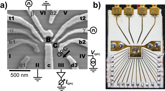
Figure 1. (a) Electron micrograph of the sample surface. Metallic gates are shown in light gray. The measuring circuit is also sketched. (b) High-frequency sample holder based on micro strip lines on a circuit board.
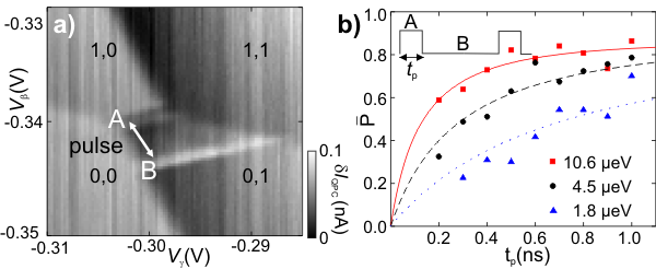
Figure 2. (a) Part of the charge stability diagram of a double quantum dot under the influence of a continuous pulse train. The pulses are applied between the points A and B in the direction of the double arrow (see also inset in (b)). (b) Probability of an electron being not in the ground state as a function of the pulse duration tp for three different interdot couplings. The coupling strength is obtained from the fit. The inset sketches the pulse train.
- D. Harbusch, S. Manus, H.P. Tranitz, W. Wegscheider and S. Ludwig, Phys. Rev. B 82, 195310 (2010).
Optical and optoelectronical phenomena in nanodevices
Spatially indirect excitons in double quantum well heterostructures were one major topic of our optical studies. On InGaAs-based heterostructures we realized a new type of electrostatic gate-defined trap for indirect excitons in which the exciton generation is spatially separated from the trapping potential. Thus the trap is filled only with indirect excitons which are pre-cooled to the lattice temperature. We employed spatially resolved luminescence to demonstrate full control of the in-plane dynamics of the exciton ensemble. Studying indirect excitons in GaAs double quantum wells we found that under conditions of resonant excitation a highly efficient initialization of the exciton spin takes place and identified long spin relaxation times for indirect excitons. We further showed that both formation and trapping of spatially indirect dipolar excitons in the illumination spot are dramatically enhanced by applying a magnetic field perpendicular to the quantum well plane. Both, dipolar exciton densities and excess hole densities could be deduced from magnetic field evolution of the spectra. Individual semiconducting carbon nanotubes were another major research topic. Here we established methods of identifying and visualizing carbon nanotubes by complementary imaging techniques: scanning electron microscopy, atomic force microscopy and confocal cryogenic photoluminescence microscopy. Observation of field induced energy shifts, generated by static electric fields applied perpendicular to the nanotube axis and exceeding the spectral linewidth indicate that emission properties of carbon nanotubes can be controllably tuned using the quantum confined Stark effect.
Electrostatically trapping indirect excitons in coupled InGaAs quantum wells
Georg J. Schinner, Enrico Schubert, Markus P. Stallhofer and J. P. Kotthaus
in collaboration with Andreas D. Wieck and Alexander O. Govorov
We introduce a new type of electrostatic gate-defined trap for spatially indirect excitons (IX). In this trapping configuration, the exciton generation is spatially separated from the trapping potential. Thus the exciton trap is filled only with indirect excitons, pre-cooled to the lattice temperature. This is in contrast to the majority of traps previously realized. Using spatially resolved photoluminescence (PL) we demonstrate the operating principle as shown in Fig. 1. We are able to fully control the in-plane exciton gas dynamics by suitable chosen voltages applied to the gates. We show how each gate influence the exciton behavior when the applied bias is changed. Additionally, it is possible to use a non-linear trapping configuration to switch the exciton population and we present the characteristics of switching the IX flow. Furthermore, we observe and interpret an unexpected nonlinear increase of the PL intensity with the trapped IX density [1].
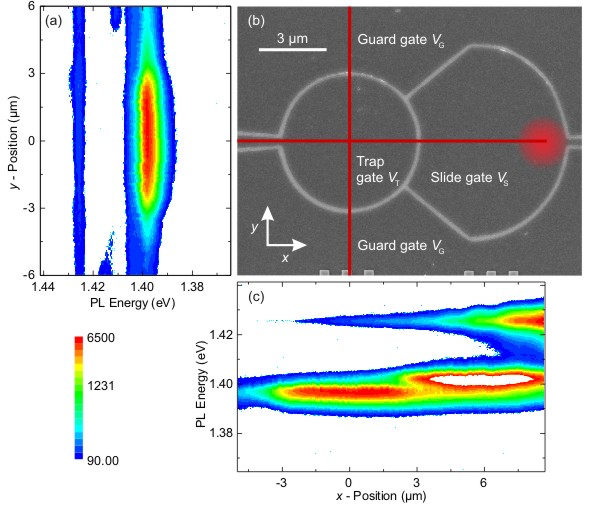
Figure 1. The figure shows spatially and energy-resolved measurements of the excitonic PL distribution in the "chute" trap at 4K. In (a) and (c) cuts are shown of the PL intensity in a logarithmic color scale, given by the scale bar on the lower left, as a function of the position and PL energy. The data are measured along the red lines in the scanning electron micrograph shown in (b) of the trapping configuration which is composed of a slide, trap and guard gate. The pump laser is operated continuously at 1.494 eV with 8.0 µW incident power and its position is fixed on the slide gate as indicated by the bright spot in (b).
- G.J. Schinner, E.Schubert, M.P. Stallhofer, D.Schuh, A.K. Rai, D. Reuter, A.D. Wieck, A.O. Govorov and J.P Kotthaus, Phys. Rev. B 83, 165308 (2011), Phys. Rev. B 83, 165308 (2011).
Long exciton spin relaxation in coupled quantum wells
Katarzyna Kowalik-Seidl, Xaver P. Vögele, Bernhard Rimpfl, Stephan Manus and Jörg P. Kotthaus,
in collaboration with Dieter Schuh and Alexander W. Holleitner
The spin memory of indirect excitons in coupled GaAs double quantum well is investigated via time- and polarization-resolved photoluminescence (PL) studies after resonant and non-resonant excitation of the direct and indirect exciton states [1]. We observe that under conditions of resonant excitation a highly efficient initialization of exciton spin takes place (compare Fig. 1 a-b). The PL circular polarization can be simply written as Pcirc = P0 s /(s + r) where s (r) is the spin relaxation time (radiative lifetime) of excitons and P0 is the effective initial circular polarization determined by the laser polarization and losses during the formation of an indirect exciton. Hereby, we estimate that the spin relaxation under strictly resonant excitation is at least 1.2 times longer than the exciton lifetime, when neglecting any polarization loss in the excitation process P0 = 1. The radiative lifetime for indirect excitons reaches several tens of nanoseconds, thus the spin relaxation time must be even longer.
To confirm this hypothesis we apply a pulsed excitation at 1.577 eV and "co" or "cross" polarized photoluminescence spectra are recorded for different delays after the 400 ns long laser pulse. The PL remains strongly circularly polarized long after the laser pulse and nearly constant during the lifetime of excitons (see Fig. 1 c). Our results directly confirm a long spin relaxation time of > 80 nanoseconds for indirect excitons.
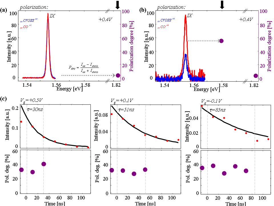
Figure 1.PL spectra for indirect excitons (IX) under nonresonant excitation (a) under resonant 1.58 eV excitation (b), polarization resolved in "co" (blue) and "cross" (red) configurations. Right scale: degree of circular polarization for indirect excitons vs. excitation laser energy (violet). The gray arrows indicate the point obtained from the spectra shown in the left part of the figure. (c) For three different applied biases under 1.577 eV excitation: upper part - PL decay vs. delay time after the excitation pulse (circles - experimental data), line - exponential fit, and lower part - circular polarization degree. Vertical dashed lines mark zero delay and the one corresponding to the PL decay time, respectively.
- K. Kowalik-Seidl et al., Appl. Phys. Lett. 97, 011104 (2010).
Forming and confining of dipolar excitons by quantizing magnetic fields
Katarzyna Kowalik-Seidl, Xaver P. Vögele, Florian Seilmeier, Stephan Manus and Jörg P. Kotthaus,
in collaboration with Dieter Schuh and Alexander W. Holleitner
Employing confocal microscopy we experimentally show that formation and trapping of spatially indirect dipolar excitons in the illumination spot is dramatically enhanced by a quantizing magnetic field [1]. Under focused excitation a spatial non-equilibrium of photo-generated carriers forms: electrons drift out of the focus spot much faster than the much heavier holes (see Fig. 1 a). In order to suppress the electron escape one can use a magnetic field. The electron drift is modified by the circular motion caused by the Lorentz force resulting in a cycloidlike trajectory. At a threshold field B* this force dominates the electron movement, and for higher B the electrons propagate on cyclotron orbits and stay within the excitation area (Fig. 1 a). Figure 1c present the evolution of the photoluminescence (PL) in a perpendicular magnetic field. Without a magnetic field the indirect excitons radiate very weakly and the emission is dominated by the direct transition (Fig. 1c, upper branch at ~1.573 eV). Under applied magnetic field the intensity of the indirect transition increases by a factor of 10. Additionally, we note that the spectrum splits under magnetic fields and the optical transitions form a Landau level (LL) fan chart (like in scheme in Fig. 1 b). The two first LL transitions are clearly visible for indirect excitons (Fig. 1c). The difference in the filling of consecutive LLs suggests an increase of excess hole density with increasing excitation intensity. Two field regimes are clearly distinguishable for the indirect excitons. For low fields (B < B*) the transition energy shifts is dominated by the PL blue shift as expected for interacting system of dipolar excitons with increasing density. For high magnetic fields (B > B*) it can be described using a simple picture of excitonic transitions in the presence of carriers. From magnetic field evolution of the spectra we determine dipolar exciton densities and excess hole densities separately (see Fig. 1d), which depending on the applied electric field and excitation conditions reach several 1011cm-2.
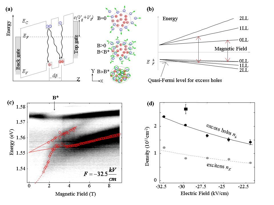
Figure 1. (a) Sketch of the band gap between conduction (EC) and valence (EV) band edge in a coupled GaAs/(Al,Ga)As double quantum well, respectively (along the growth direction Z). The applied gate voltage Vg and built-in voltage VS sum up to a electric field between the n-doped back gate and the top gate. Two different optical transitions (direct and indirect) are marked with waved arrows. Right: scheme of the in-plane (X-Y) distribution of electrons and holes at the excitation spot (big circle) for different magnetic fields. Arrows mark the diffusion of electrons. (b) Scheme of optical selection rules between electron and hole Landau levels in a perpendicular magnetic field. Dotted horizontal line marks the quasi-Fermi level (EhF) for holes. (c) Magnetic field evolution of PL spectra for different electric fields. (d) Densities vs. electric field: for excess holes (black points - series taken at excitation power P0, square - at 2P0) and for the exciton density (gray points). Solid and dashed lines are guide for eyes.
- K. Kowalik-Seidl et al., submitted for publication (2010); arXiv:1009.0427.
Photoluminescence of individual carbon nanotubes in static electric fields
Jan T. Glückert, Wolfgang Schinner, Alexander Kneer and Alexander Högele
Semiconducting single-walled carbon nanotubes (CNTs) show photoluminescence (PL) emission at near infrared wavelengths [1] due to radiative recombination of excitons [2-3]. We use cryogenic conditions to study the emission spectra of individual CoMoCat CNTs as a function of external electric field. We fabricated a sample that allows for applying static electric fields perpendicular to the nanotube axis (Figure 1) and observed spectral shifts exceeding the spectral linewidth (Figure 2, inset) with a linear dependence of the peak wavelength on the electric field strength.
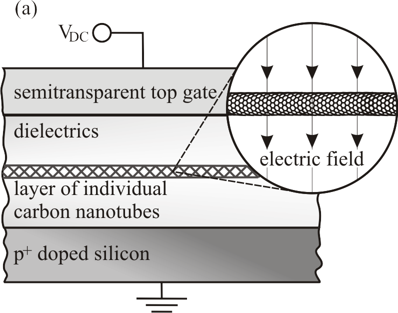
Figure 1. Gate structure with carbon nanotubes sandwiched between dielectric layers and capacitor plates formed by a highly doped silicon substrate (back gate) and a semitransparent metal layer (top gate).
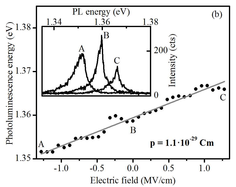
Figure 2. Photoluminescence energy shows a linear dependence on the electric field characteristic of dc Stark shift. Inset: Photoluminescence emission spectra at three different electric field values.
- M. J. O'Connell et al., Science 297, 593 (2002).
- J. Maultzsch et al., Physical Review B 72, 241402 (2005).
- F. Wang et al., Science 308, 838 (2005).
Imaging techniques for carbon nanotubes
Matthias Hofmann, Jan T. Glückert and Alexander Högele
Reliable methods of identifying and imaging carbon nanotubes (CNTs) are crucial for sample fabrication intended for optical spectroscopy of individual CNTs. We investigated CoMoCat nanotubes [1] with well established values of diameter and chirality distribution [2] by applying three complementary imaging techniques: scanning electron microscopy (Figure 1b), atomic force microscopy and confocal photoluminescence (PL) microscopy at cryogenic temperatures (Figure 1a, c). Lithographically defined metallic markers on the Si/SiO2-substrate allow for a comparative study of specific sample regions with dispersed individual nanotubes using all three methods.
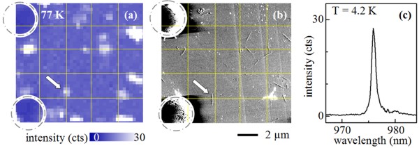
Figure 1. Imaging microscopy of carbon nanotubes: (a) Photoluminescence intensity as a function of lateral displacement showing multiple hotspots of carbon nanotube emission. (b) Scanning electron microscope image of the sample region in (a). Grid lines are drawn to support direct comparison between the two images. Grey dash-dotted circles indicate a lithographically defined reference frame on the sample surface. (c) Photoluminescence spectrum of the carbon nanotube indicated by the arrow in (a) and (b) at T = 4.2 K.
- B. Kitiyanan et al, Chem. Phys. Lett. 317, 497 (2000).
- S. M. Bachilo et al, J. Am. Chem. Soc. 125, 11186 (2003).
Nanomechanical systems
Nanomechanical systems, freely suspended nanostructures with nanoscale cross-sections and lengths of up to several 10 microns, feature a range of promising applications ranging from sensing to signal processing. In order to exploit their potential, detailed understanding of fundamental properties such as the quality factor are required. A core topic of our research are nanoresonators fabricated from amorphous high stress silicon nitride. In this material, the intrinsic stress accounts for large room temperature quality factors exceeding 100,000 at eigenfrequencies of the order of 10 MHz. High stress silicon nitride resonators can be employed to map out the highly nonlinear response regime where bistability and switching phenomena are investigated. These high Q nanoresonators are also employed in cavity nano-optomechanics where mechanical vibrations of nanoresonators are coupled to the modes of high finesse optical cavities. Both fiber-based Fabry-Perot microcavities as well as microtoroid cavities are employed, targeting ultra-sensitive displacement detection near and below the standard quantum limit as well as backaction phenomena.
Nonlinear switching dynamics in a nanomechanical resonator
Thomas Faust, Quirin P. Unterreithmeier and Jörg P. Kotthaus
Nanomechanical resonators fabricated out of high stress silicon nitride exhibit high mechanical quality factors, in the range of 105 at resonance frequencies in the order of 10 MHz. These resonators are ideal model systems to investigate the detailed mechanical properties of nano-scale objects, such as the nonlinear behaviour.
We report on a systematic study of the time-dependent response of a nanomechanical resonator driven well into the nonlinear regime [1]. Their bistable response allows their use as a simple mechanical memory element. Using a constant actuation to drive the resonator into the nonlinear regime and applying short resonant RF pulses of variable phase and duration, we are able to reach arbitrary points in the phase space of the resonator and study the time-evolution of the relaxation process.
By mapping out the corresponding final state for different pulse parameters, we are able to demonstrate quantitative agreement with our perturbation calculation (Fig 1). Our detailed understanding allows us to determine the parameters required to actively switch directly between the stable states. We experimentally demonstrate that switching thus becomes possible on time scales much shorter than the relaxation time of the resonator (Fig 2). This opens the pathway towards integrated large-scale nanomechanical memory elements once completely electrical on-chip detection has been implemented.
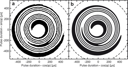
Figure 1. Measured (a) and simulated (b) final state after the application of pulses with varied phase and duration, starting from the low amplitude state and ending in the high (black) or low (white) amplitude state.
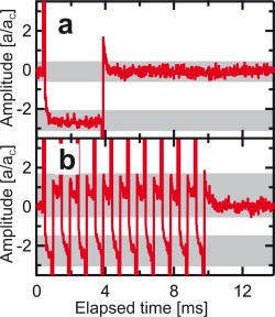
Figure 2. Time-resolved switching between the two stable states highlighted by the grey bars, a) showing no relaxation oscillations, b) demonstrating a repetition rate of 1 kHz.
- Q. Unterreithmeier, T. Faust, J.P. Kotthaus, Phys. Rev. B 81, 241405(R) (2010).
Quality Factors of Nanomechanical Resonators
Thomas Faust, Quirin P. Unterreithmeier and Jörg P. Kotthaus
In this work, we systematically studied the damping of prestressed silicon nitride resonators in order to gain insight into the underlying physical mechanisms.
Measuring the room-temperature quality factors of the fundamental and higher harmonic modes of high stress SiN nanomechanical oscillators with cross sections of 200x100 nm and lengths ranging from 35 to 5 micrometer, we find a strong mode dependence of the quality factor [1]. This can be explained by applying a damping model based on continuum mechanics.
Assuming the friction throughout volume of the resonator to be caused by the local strain variations as the beam oscillates, we are able to quantitatively model the observed quality factors introducing a frequency-independent imaginary part of the Youngs modulus (Fig. 1). Based on our calculations we can deduce that the high mechanical quality factors are caused by the increase in elastic energy rather than a decrease in energy loss with increasing tensile stress. Therefore, we expect that resonators consisting of nearly any material will exhibit higher quality factors when stressed.
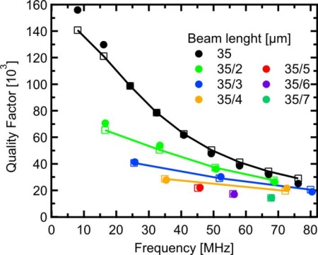
Figure 1.Frequency and mechanical quality factors of the measured resonances (solid dots); the lengths of the beams are colour-coded. The hollow squares represents our modelling of the resonance frequencies as well as the quality factors. As a guide to the eye, the various harmonics corresponding to the same beam are connected.
- Q. Unterreithmeier, T. Faust, J.P. Kotthaus, Phys. Rev. Lett. 105, 027205 (2010).
Cavity nano-optomechanics: a nanomechanical system in a high finesse optical cavity
Sebastian Stapfner, Phillip Paulitschke, Heribert Lorenz and Eva M. Weig,
in collaboration with Ivan Favero (Paris Diderot), David Hunger (LMU), Jakob Reichel (ENS) and Khaled Karraï (LMU)
The coupling of mechanical oscillators with light has seen a recent surge of interest, as recent reviews report. This coupling is enhanced when light is confined in an optical cavity where the mechanical oscillator is integrated as backmirror or movable wall. At the nano-scale, the optomechanical coupling increases further thanks to a smaller optomechanical interaction volume and reduced mass of the mechanical oscillator.
We have employed our cavity nano-optomechanics setup based on a sub-wavelength sized mechanical resonator coupled to a high finesse optical microcavity to optically map out the driven response of mechanical nanoresonators [1]. The vibrational resonances of a series of piezo-actuated EBD-grown carbon nanorods were first characterized in an optical microscope (Fig. 1). Using the optical cavity as a transducer of nanomechanical motion, we optically monitor the piezo-driven nanorod vibration with a much higher precision (Fig. 2). In principle this set-up combining a miniature Fabry-Pérot cavity with a nanomechanical resonator is applicable to studying light-induced backaction effects.
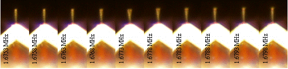
Figure 1. Series of optical microscope images of an EBD nanorod vibrating resonantly at 1.677 MHz. The micrographs taken during the frequency scan across the resonance illustrate the respective change in amplitude. The excitation frequency is indicated on each picture.
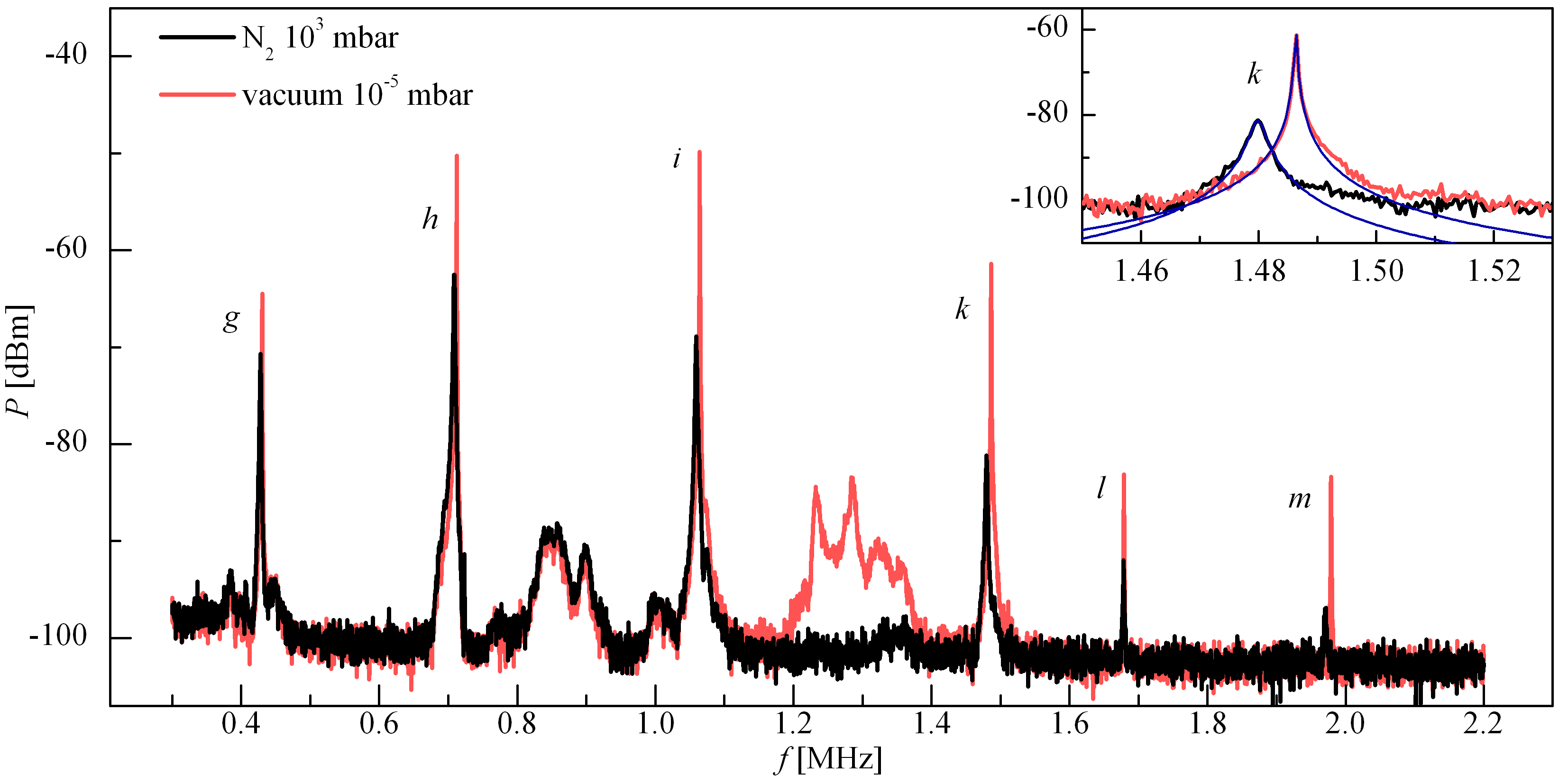
Figure 2. Noise spectrum of the optical cavity reflectivity showing the vibrational modes of the actuated nanorod positioned in the cavity mode. Measurements are carried out in nitrogen at atmospheric pressure (black line) and in vacuum at 10-5 mbar (red line). The inset gives a close-up on resonance k showing the different response in N2 and vacuum. The blue lines are Lorentzian fits to the individual resonances.
- S. Stapfner et al., Proceedings of SPIE Vol. 7727, 772706 (2010).
Measuring nanomechanical motion with an imprecision below the standard quantum limit
Quirin P. Unterreithmeier, Eva M. Weig and Jörg P. Kotthaus,
in collaboration with Georg Anetsberger (MPQ), Emanuel Gavartin (EPFL), Olivier Arcizet (MPQ), Michael L. Gorodetsky (Moscow State University) and Tobias J. Kippenberg (MPQ)
In a second cavity nano-optomechanics experiment, the radiation pressure coupling between the vibrational modes of a high Q silicon nitride nanostring and an ultra high finesse silica microtoroid cavity has been explored. In this hybrid approach, cavity-enhanced near field coupling is realized by approaching the nanomechanical resonator well into the evanescent field of the toroid's whispering gallery modes. In order to increase the resulting coupling rates, both toroid diameter and optical wavelength have been reduced. The total imprecision of 530 am/√Hz, corresponding to 3 dB below the standard quantum limit (SQL), is limited by fundamental thermorefractive cavity noise at room temperature which is expected to reduce to negligible values at moderate cryogenic temperatures. Coupling strengths exceeding those required to reach the SQL by more than two orders of magnitude are achieved, allowing a shot-noise limited imprecision more than 10 dB below the SQL (Fig. 1). The transducer, thus, in principle, allows access to the quantum backaction dominated regime, a prerequisite for exploring quantum backaction, measurement-induced squeezing, and obtaining sub-SQL sensitivity using backaction evading techniques.
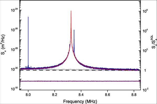
Figure 1. Shot-noise limited imprecision more than 10 dB below the SQL. The total measurement imprecision is approximately at the SQL. The shot-noise level (gray, lower line), however, lies more than 10 dB lower at Sx = (250 am/√Hz)2 = 0.09 SxSQL.
- G. Anetsberger et al., Phys. Rev. A 82, 061804(R) (2010).
Bachelor theses completed in 2010
- Maximilian Freiermuth
“Spektroskopie an selbstorganisierten Quantenpunkten” - Alexander Kneer
“Effects of Static Electric Fields on the Emission Spectrum of Carbon Nanotubes”
Diploma theses completed in 2010
- Matthias Benecke
“Untersuchungen an Quantenpunktkontakten im Hinblick auf 0.7-Anomalie” - Bernhard Rimpfl
“Die Dynamik von indirekten Exzitonen in elektrostatisch definierten Potentiallandschaften in GaAs/AlGaAs-Doppelquantentöpfen” - Enrico Schubert
“Elektrostatische Fallen für indirekte Exzitonen in gekoppelten InGaAs-Quantentöpfen” - Lukas Ost
“Kontrolliertes Wachstum von Kohlenstoffnanoröhrchen für optomechanische Experimente” - Matthias Hofmann
“Wachstum und Charakterisierung von Kohlenstoff-Nanoröhren” - Max Empl
“Radiofrequenzspektroskopie an tunnelgekoppelten Dreifachquantenpunkten” - Norbert Seltner
“Mechanische Eigenschaften nanostrukturierter GaAs-Säulen”
PhD theses completed in 2010
- Dawid Kupidura
“Spinwechselwirkung eines Doppelquantenpunkts mit dem Kernfeld. Anpassschaltung für einen rf-Quantenpunktkontakt” - Xaver Vögele
“Indirekte Exzitonen in elektrostatisch de?nierten Potentiallandschaften” - Matthias Fiebig
“Spatially resolved electronic and optoelectronic measurements of pentacene thin film transistors” - Quirin Unterreithmeier
“Gradient Field Transduction of Nanomechanical Resonators”
Guest scientists in 2010
- Prof. Alexander Holleitner
Technische Universität München, Walter Schottky Institut - Prof. Khaled Karraï
Technische Universität München - Prof. Alexander O. Govorov
Ohio University, Athens, OH, USA, SFB 631 - Prof. Valeri Dolgopolov
Russian Academy of Sciences, Chernogolovka, Russia, Alexander von Humboldt Stiftung - Dr. Katarzyna Kowalik
Grenoble High Magnetic Field Laboratory, Grenoble, France, Alexander von Humboldt Stiftung - Dr. Eric Hoffmann
Physics Department & Material Science Institute, University of Oregon, USA, Alexander von Humboldt Stiftung - Prof. Dr. Mansour Shayegan
Princeton University, USA, Alexander von Humboldt Stiftung
Group members in 2010
Senior scientists
- Prof. Jörg P. Kotthaus
- Prof. Alexander Högele
- Dr. Heribert Lorenz
- Dr. Stefan Ludwig
- Dr. Eva-Maria Weig
- Dr. Felix Mendoza
- Dr. Constanze Metzger
Secretary
- Martina Jüttner
Technical staff
- Philipp Altpeter
- Hans-Peter Kiermaier
- Wolfgang Kurpas
- Stephan Manus
- Reinhold Rath
Ph.D. students
- Thomas Faust
- Matthias Fiebig
- Jan Tibor Glückert
- Daniel Harbusch
- Dawid Kupidura
- André Neumann
- Philipp Paulitschke
- Gunnar Petersen
- Johannes Rieger
- Georg Schinner
- Florian Seilmeier
- Sebastian Stapfner
- Daniela Taubert
- Xaver Vögele
- Quirin Unterreithmeier
Diploma students
- Matthias Benecke
- David Borowsky
- Max Empl
- Felix Donhöfner
- Matthias Hofmann
- Peter Krenn
- Lukas Ost
- Bernhard Rimpfl
- Enrico Schubert
- Norbert Seltner
Publications in 2010
- D. V. Scheible and R. H. Blick
“A mode-locked nanomechanical electron shuttle for phase-coherent frequency conversion”
New Journal of Physics 12, 023019 (2010). - Matthias Fiebig, Daniel Beckmeier and Bert Nickel
“Thickness-dependent in situ studies of trap states in pentacene thin film transistors”
Applied Physics Letters 96, 083304 (2010). - Quirin P. Unterreithmeier, Thomas Faust, Stephan Manus and Jörg P. Kotthaus
“On-Chip Interferometric Detection of Mechanical Motion”
Nano Letters 10, 887 (2010). - David Hunger, Stephan Camerer, Theodor W. Hänsch, Daniel König, Jörg P. Kotthaus, Jakob Reichel and Philipp Treutlein
“Resonant coupling of a Bose-Einstein condensate to a Micromechanical Oscillator”
Phys. Rev. Lett. 104, 143002 (2010). - D. Harbusch, D. Taubert, H.P. Tranitz, W. Wegscheider and S. Ludwig
“Phonon-mediated vs. Coulombic Back-Action in Quantum Dot circuits”
Phys. Rev. Lett. 104, 196801 (2010). - Quirin P. Unterreithmeier, Thomas Faust and Jörg P. Kotthaus
“Nonlinear Switching Dynamics in a Nanomechanical Resonator”
Phys. Rev. B 81, 241405 (2010). - S. Stapfner, I. Favero, D. Hunger, P. Paulitschke, J. Reichel, K. Karraï and E. M. Weig
“Cavity nano-optomechanics: a nanomechanical system in a high finesse optical cavity”
Proc. SPIE 7727, 772706 (2010). - K. Kowalik-Seidl, X. P. Vögele, B. N. Rimpfl, S. Manus, J. P. Kotthaus, D. Schuh, W. Wegscheider and A. W. Holleitner
“Long exciton spin relaxation in coupled quantum wells”
Appl. Phys. Lett. 97, 011104 (2010). - C. Rössler, M. Herz, M. Bichler, S. Ludwig
“Freely suspended quantum point contacts”
Solid State Communications 150, 861 (2010). - Quirin P. Unterreithmeier, Thomas Faust and Jörg P. Kotthaus
“Damping of Nanomechanical Resonators”
Phys. Rev. Lett. 105, 027205 (2010). - Klaus-Dieter Hof, Franz J. Kaiser, Markus Stallhofer, Dieter Schuh, Werner Wegscheider, Peter Hänggi, Sigmund Kohler, Jörg P. Kotthaus and Alexander W. Holleitner
“Spatially Resolved Ballistic Optoelectronic Transport Measured by Quantized Photocurrent Spectroscopy”
Nano Letters 2010, 10, 3836 (2010). - D. Taubert, G. J. Schinner, H. P. Tranitz, W. Wegscheider, C. Tomaras, S. Kehrein
and S. Ludwig
“An electron avalanche amplifier based on the electronic Venturi effect”
Phys. Rev. B 82, 161416 (2010). - A. Siddiki, J. Horas, D. Kupidura, W. Wegscheider and S. Ludwig
“Asymmetric non-linear response of the quantized Hall effect”
New Journal of Physics 12, 113011 (2010). - D.Harbusch, S. Manus, H.P. Tranitz, W. Wegscheider and S. Ludwig
“Radio frequency pulsed-gate charge spectroscopy on coupled quantum dots”
Phys. Rev. B 82, 195310 (2010). - A. Wild, J. Sailer, J. Nützel, G. Abstreiter, S. Ludwig and D. Bougeard
“Electrostatically defined quantum dots in a Si/SiGe heterostructure”
New Journal of Physics 12 (2010) 113019. - M.G. Prokudina, V.S. Khrapai, S. Ludwig, J.P. Kotthaus, H.P. Tranitz and W. Wegscheider
“Acoustic-phonon-based interaction between coplanar quantum circuits in a magnetic field”
Phys. Rev. B 82, 201310 (2010). - K.-D. Hof, C. Rössler, S. Manus, J.P. Kotthaus, A.W. Holleitner, D. Schuh, W. Wegscheider
“Photoconductive gain in semiconductor quantum wires”
AIP conf. Proc. 1199, 331 (2010). - G. Anetsberger, E. Gavartin, O. Arcizet, Q.P. Unterreithmeier, E.M. Weig, M.L. Gorodetsky, J.P. Kotthaus and T.J. Kippenberg
“Measuring nanomechanical motion with an imprecision below the standard quantum limit”
Phys. Rev. A 82, 061804 (2010).
Invited talks in 2010
Jörg P. Kotthaus
- “Nanomechanical resonators”
5th Windsor Summer School "Quantum Phenomena in Low-Dimensional Materials and Nanostructures"
Windsor, United Kingdom
August 2010
- “Efficient transduction to nanomechanical resonators via electrical and optical gradient forces”
2010 RBNI Winter School in Nanoscience and Nanotechnology
Ein Gedi, Israel
February 2010
Eva M. Weig
- “Gradient force transduction and self-oscillation of nanomechanical resonators”
International Symposium on Advances in Nanoscience
Garching
October 2010
- “Voltage-sustained self-oscillation of a nanomechanical electron shuttle”
Workshop "Nano-Opto-Electro-Mechanical Systems Approaching the Quantum Regime"
Triest, Italy
September 2010
- “Gradient force transduction and self-oscillation of nanomechanical resonators”
Workshop "Physics of Hearing and Neurons meets Nanoelectromechanics"
Asia Pacific Center for Theoretical Physics (APCTP), Pohang, Southkorea
August 2010
- “Charge transport and self-oscillation of a nanomechanical shuttle”
30th International Conference on the Physics of Semiconductors (ICPS)
Seoul, Southkorea
July 2010
- “Gradient force transduction and self-oscillation of nanomechanical resonators”
Symposium "Hybrid Quantum Systems: New Perspectives for Quantum State Control"
Heidelberg
May 2010
- “Gradient force transduction and self-oscillation of nanomechanical resonators”
Gordon Conference "Mechanical Systems in the Quantum Regime"
Galveston, USA
March 2010
- “Gradient force transduction, self-oscillation and electron shuttling with nanomechanical systems”
International Symposium "Quantum Nanostructures and Spin-related Phenomena (QNSP)"
Tokio, Japan
March 2010
Daniela Taubert
- “An electron jet pump based on the Venturi effect in a Fermi liquid”
30th International Conference on the Physics of Semiconductors (ICPS)
Seoul, Southkorea
July 2010
Alexander Högele
- “Locking of the quantum dot electron-nuclear spin system to a resonant laser”
APS March Meeting 2010
Portland, OR, USA
March 2010
Stefan Ludwig
- “Tunnelling Systems on Demand: Playing with Few Electrons on the Nanoscale”
Symposium: From Superfuid 3He to Glasses: Snapshots of Matter at Low Temperatures
Stanford, USA
October 2010
- “Indirect Back-Action in Quantum Dot Circuits”
30th International Conference on the Physics of Semiconductors (ICPS)
Seoul, Korea
July 2010
- “Non-Equilibrium Interactions on the Nanoscale: An Electron-Jet Pump Illuminates Back-Action in Quantum Dot Circuits”
37th International Symposium on Compound Semiconductors (ISCS)
Takamatsu (Kagawa), Japan
June 2010
- “Phonon-Mediated vs. Coulombic Back-Action in Quantum Dot Circuits”
16th International Winterschool Mauterndorf: New Developments in Solid State Physics
Mauterndorf, Austria
February 2010
- “Phonon-Mediated vs. Coulombic Back-Action in Quantum Dot Circuits”
IAP Workshop on Semiconductor Quantum Dots and Nanowires
Louvain-la-Neuve, Belgium
January 2010
Senior scientists of cooperating groups
- Gerhard Abstreiter∗, Max Bichler, Dominique Bougeard
Walter Schottky Institut, TU München, Garching, Germany. - Robert Blick
University of Wisconsin-Madison, USA. - Alik Chaplik
Institute of Semiconductor Physics, Novosibirsk, Russia. - Valeri Dolgopolov, Vadim Khrapay
Russian Academy of Sciences, Chernogolovka, Russia. - Ivan Favero
Université Paris Diderot, France. - Niels Fertig+
Nanion GmbH, München, Germany. - Hermann Gaub∗+
LMU München, Germany. - Geza Giedke
Max-Planck Institute for Quantum Optics, Garching, Germany. - Alexander O. Govorov
Ohio University, Athens, OH, USA. - Peter Hänggi∗
Universität Augsburg, Germany. - Theodor W. Hänsch∗, Philipp Treutlein
LMU München, Germany and Max-Planck Institute for Quantum Optics, Garching, Germany. - Achim Hartschuh∗+
LMU München, Germany. - Wolfgang Heckl∗+
LMU München, Germany. - Moty Heiblum
Weizmann Institute of Science, Rehovot, Israel. - Alexander Holleitner∗+
Walter Schottky Institut, TU München, Garching, Germany. - Peter Hommelhoff
Max-Planck Institute for Quantum Optics, Garching, Germany. - Atac Imamoglu
Department of Physics, ETH Swiss Federal Institute of Technology, Zürich, Switzerland. - Khaled Karraï+
attocube Systems and LMU München, Germany. - Stefan Kehrein∗+
LMU München, Germany. - Tobias Kippenberg∗
Max-Planck Institute for Quantum Optics, Garching, Germany and École Polytechnique Fédérale de Lausanne, Switzerland. - Don Lamb∗+
LMU München, Germany. - Tim Liedl∗+
LMU München, Germany. - Efrat Lifschitz
Technion, Haifa, Israel. - Ron Lifschitz
Tel Aviv University, Israel. - Bernd Löchel
Helmholtz-Zentrum für Materialien und Energie, Berlin, Germany. - Axel Lorke+
Universität Duisburg-Essen, Germany. - Paolo Lugli∗
TU München, Germany. - Florian Marquardt∗+
Universität Erlangen, Germany. - Pierre M. Petroff
University of California - Santa Barbara, USA. - Joachim Rädler∗+, Doris Heinrich+, Bert Nickel∗+
LMU München, Germany. - Jakob Reichel
École normale supérieure, Paris, France. - Andrew Sachrajda
Institute for Microstructural Sciences, National Research Council, Ottawa, Canada. - Lukas Schmidt-Mende∗+
LMU München, Germany. - Dieter Schuh
Institut für Angewandte und Experimentelle Physik, Universität Regensburg, Germany. - Mansour Shayegan
Princeton University, USA. - Afif Siddiki
Mugla University, Turkey. - Friedrich Simmel∗+
TU München, Garching, Germany. - Christoph Strunk
Institut für Angewandte und Experimentelle Physik, Universität Regensburg, Germany. - Jan von Delft∗+
LMU München, Germany. - Richard Warburton
Heriot-Watt University, Edinburgh, U.K. and Universität Basel Switzerland. - Werner Wegscheider
Department of Physics, ETH Swiss Federal Institute of Technology, Zürich, Switzerland. - Andreas Wieck, Dirk Reuter
Ruhr-Universität Bochum, Germany. - Ignacio Wilson-Rae
TU München, Garching, Germany. - Achim Wixforth∗+
Universität Augsburg, Germany.
+ Member of the Nanosystems Initiative Munich (NIM)
Financial support in 2010
Funding of this work via the following agencies is gratefully acknowledged:
- Alexander von Humboldt - Stiftung
- Bayerisch-Kalifornisches Hochschulzentrum (BaCaTeC)
- Bundesministerium für Bildung und Wissenschaft, Forschung und Technologie (BMBF)
- Deutscher Akademischer Austausch Dienst
- PROCOPE Programm
- Deutsche Forschungsgemeinschaft
- European Union
- German-Israeli Foundation for Scientific Research and Development
- Ludwig-Maximilians-Universität München
- Robert Bosch Stiftung
- Volkswagen Stiftung