

Research report 2006
- Introduction
- Electronic properties
- Kondo effect in a one electron double quantum dot
- A double-dot quantum ratchet driven by an independently biased quantum point contact
- A lateral serial few-electron triple quantum dot
- Manipulation of the spin of a single electron
- Freely suspended quantum dots
- Quantum mechanical switching of ballistic electrons
- Strain-dependent electrical transport in carbon nanotubes
- Spatially resolved photoresponse measurements on pentacene thin film transistors
- Optics with nanostructures
- Nanomechanical systems
- Nanobioscience
- Diploma theses in 2006
- PhD theses in 2006
- Habilitations in 2006
- Guest scientists in 2006
- Group members in 2006
- Publications in 2006
- Invited talks in 2006
- Senior scientists of cooperating groups
- Financial support in 2006
Introduction
Nanoscale devices and systems continue to be the major subject of our research. In our work we combine the realization and study of top-down fabricated devices employing techniques derived from semiconductor processing with the exploration of bottom-up assembled systems made via chemical and biochemical routes. Our goals range from a deeper fundamental understanding of physical behavior in the nanometer regime to the realization of novel devices, functions, and systems utilizing a variety of nanotechnologies.
Our studies of electronic properties of nanoscale systems aim at exploring the effects of quantum confinement and many-body interactions on electronic behavior and their potential for applications in processing information. One ongoing major research theme are ways to implement and control quantum bits on the basis of solid state electronic and optical devices and thus lay the ground work for a future quantum information technology. In part this research is embedded in the SFB 631 - a long-term research platform on ”Solid-State Based Quantum Information Processing”, supported by the German Science Foundation (DFG) since July 2003. In addition we participate in a research program on ”Nanoelectronic semiconductor structures for the quantum information technology” (NanoQuit) funded since January 2005 by the German Ministry for Education and Research (BMBF) with research on ”Quantum control in suspended semiconductor nanostructures” (QuBridge). These experiments are complemented by studies of electronic transport in molecular devices including carbon nanotubes and organic compounds.
Optical characterization and control of individual self-assembled quantum dots continue to be an important part of our activities in the field of nanooptics. This work is based on a continuous collaboration with the groups of Pierre Petroff at UC Santa Barbara and Richard Warburton at Heriot-Watt University in Edinburgh and aims at studying and controlling spin and charge quantum states with optical techniques. The dynamics of long-living excitons created in double quantum wells and moving in a controlled artificial potential landscape is another aspect of our nanooptical studies. These experiments aim at understanding many-body interactions in excitonic condensates and at the realization of Bose-Einstein condensation in excitonic systems.
In the nanometer regime electronic, mechanical and optical properties become often inseparably connected. This motivates our experiments on Nano-Electro-Mechanical Systems, in short NEMS. Ways to efficiently drive such nanoscale resonators by electric, magnetic, mechanic as well as optically induced forces are one current research aspect. Sensing the mechanical motion with nanometer resolution via capacitance, current or optical reflection is another basic theme of ongoing research.
Our investigations in the area of nanobioscience, directed by Friedrich Simmel, heading a DFG-funded Emmy-Noether junior group, successfully aim at creating artificial nanomachines by combining bottom-up biochemical assembly routes with top-down fabrication. DNA-templated and genetically controlled assembly is combined with top-down fabrication to realize and study chemically and electrodynamically driven nanodevices and -machines. The recognition received by his outstanding research is not only reflected by many invited talks at international meetings but also by several offers of tenured professor positions with a decision anticipated in 2007 as to where he will move with his group.
After substantial changes in the composition of our group in the previous years 2006 has been somewhat quieter. Alex Holleitner was appointed as junior professor in September of 2006. With the commercial success and steady growth of attocube systems, a spin-off company cofounded by Khaled Karrai and Dirk Haft, Khaled Karrai finally decided to join the company full time as Chief Research Officer but will continue to creatively interact with our research group at LMU in joined scientific research projects. After completing his Ph. D. at Ecole Normale Superieur in Paris Julien Gabelli joined us in 2006 for several months as Alexander von Humboldt fellow before accepting an attractive tenure-track offer in Paris. After successfully finishing his Alexander von Humboldt fellowship Vadim Khrapai returned to his lab at Chernogolovka and Ivan Favero, also from ENS Paris, extended his fellowship stay at LMU. In addition it was our pleasure to host again Alik Chaplik, Valeri Dolgopolov, Sasha Govorov, Mansour Shayegan, and Richard Warburton as visiting professors and Andrew Greentree as visiting researcher from Melbourne. As part of their thesis work we enjoyed the visits of Chia-Ling Chung from Dresden and Louis Gaudreau from Ottowa.
In 2006 three diploma students and three doctoral students completed their degree whereas eleven new diploma and five doctoral students joined us. Members of our group presented 11 invited talks at international conferences and workshops and published 26 papers in internationally acknowledged journals. Last not least we were very glad that our work was recognized by the success of our competition in the excellence initiative of the German government. In October 2006 the research cluster ”Nanosystems Initiative Munich” (NIM) in which we actively participate was selected and funded for five years as one of 15 German cluster of excellence covering all fields of sciences.
It is my pleasure to thank all group members for their enthusiasm and their excellent research and to thank our funding agencies for their continued generous support. We hope that many readers worldwide enjoy this report and are happy to receive any feedback.
Munich, May 7th, 2007
Jorg P. Kotthaus
Electronic properties
Reducing the length scales of transistors well below 100 nanometers is one of the present key efforts in semiconductor industry. At the same time such tiny structures allow the observation of phenomena obeying the fundamental laws of quantum mechanics. In our clean room we fabricate a variety of gate-controlled devices by e-beam lithography starting from GaAs/AlGaAs heterostructures that contain a two-dimensional electron system. One of our main efforts aims at possible applications in quantum information technology of interacting zero-dimensional quantum dots (QD). In 2006 we completed an experiment on the Kondo effect of one or two electrons charging a double QD. We are thankful for collaborations with Mikhail Kiselev (Trieste, Italy) and Boris Altshuler (New York, USA), who helped to interpret the observations. In another project we realized a quantum ratchet based on a double QD. The energy source was a strongly biased quantum point cantact in an electrically isolated circuit. Based on our previous work on double QDs, we realized in 2006 a serial triple QD and demonstrated full control of its quantum mechanical states in the regime of few electrons charging the device. A triple QD is an important step towards a full-scale quantum computer. In this still ongoing work we profit strongly from collaborations with the Lloyd Hollenberg group (Melbourne, Australia) and the Andy Sachrajda group (Ottawa, Canada). In an effort to understand the interaction between discrete electronic states and discrete vibrational modes we also explore electronic transport through double quantum dots defined in a mechanical nanoscale bridge. In addition we explore electronic transport properties in molecular devices. In 2006 one aspect were studies of the influence of mechanical strain on the conductance of individual carbon nanotubes. Another topic concerned the conductance mechanisms of organic field effect transistors based on pentacene. In close collaboration with the group of Bert Nickel we studied the interband photoresponse with high spatial resolution to obtain a better understanding of the separation of photoexcited carriers.
Kondo effect in a one electron double quantum dot
Daniel M. Schröer, Andreas K. Hüttel, and Stefan Ludwig, in collaboration with Boris L. Altshuler, Karl Eberl, Mikhail N. Kiselev
We have investigated the Kondo effect on a double quantum dot (DQD) (Fig. 1b) in the few electron limit (Fig. 1a and c). For a charge of just one electron in the DQD, our measurements display a surprising quasi oscillation of the Kondo current in dependence of a small perpendicular magnetic field of a few mT (Fig. 2). We assign this behaviour to a fine tuning of the single dot eigen-energies. The interdot tunnel coupling and, as a consequence, the Kondo current have a local maximum for perfect alignment of two orbital states of the two adjacent quantum dots. In the two-electron case, transport is determined by symmetric and anti-symmetric combinations of the wave functions (i.e. singlet and triplet). Therefore, the two-electron Kondo conductance is not sensitive to single electron eigen energies and no oscillating behavior appears (Fig. 2 inset).
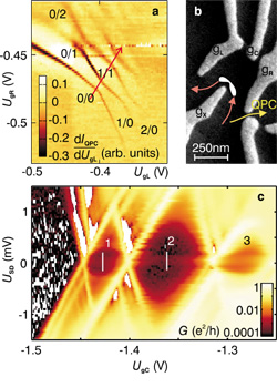
Figure 1. Stability diagram and Coulomb diamonds. (a) Stability diagram of the DQD shown in b. Colorscale plot of the transconductance dIQPC/dUgL measured using the nearby QPC. A background is subtracted for clarity. Numerals denote the number of electrons charging the (left/right) QD. (b) SEM micrograph of the top gates on the sample surface. Arrows mark possible current paths. The estimated DQD geometry is sketched in white and the nearby QPC indicated. (c) Differential conductance dI/dUSD measured through the symmetrically charged DQD as a function of bias voltage USD and center gate voltage UgC. The variation of UgC approximately corresponds to the path in the stability diagram indicated by an arrow in a. Numerals indicate the number of electrons on the DQD.
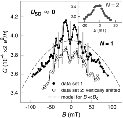
Figure 2. Non-monotonic magnetic field dependence of the Kondo effect in a one electron DQD. The inset and the main figure plot data for N=2 and N=1, respectively. One data set (open circles) is vertically shifted for clarity. The dashed curve describes the limit B << B K for N=1. Vertical lines mark local minima of the N=1 KDC.
A double-dot quantum ratchet driven by an independently biased quantum point contact
Vadim S. Khrapai, Stefan Ludwig, and Jörg P. Kotthaus, in collaboration with Werner Wegscheider
We studied a double quantum dot (DQD) coupled to a strongly biased quantum point contact (QPC), each embedded in independent electric circuits. A SEM-picture of the gate layout is shown in Fig.1a and a sketch of the experiment in Fig.1b. If the QPC is unbiased, we observe a finite current through the DQD only at the triple points of its charge stability diagram, where Coulomb blockade is lifted. This situation is plotted in Fig.1c. For a strong bias on the QPC and weak interdot tunneling of the DQD we observe a finite current flowing even through the Coulomb blockaded DQD (Fig.1d). The direction of the current through the DQD is determined by the relative detuning of the energy levels of the two quantum dots. We interpret the results in terms of a quantum ratchet phenomenon in a DQD energized by a nearby QPC. The QPC emits energy quanta, which can be reabsorbed by the DQD as sketched in the inset of Fig.1d. For the sketched case electrons are pumped through the DQD from the right lead to the left lead.
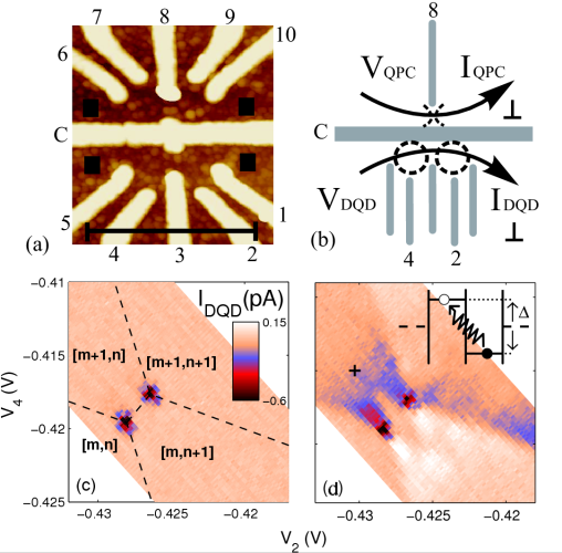
Figure 2.(a) AFM micrograph of the sample. Metal surface gates have a light color. Black squares mark source and drain regions. The black scale bar marks a length of 1 µm. (b) Schematic layout of the device as used for the ratchet experiment. The QPC is defined in the upper circuit and the DQD in the lower half. (c) DQD stability diagram for VDQD = 20 µV and an unbiased QPC. The axes show gate voltages on the plunger gates 2 and 4. (d) Same area of the stability diagram as in (c), but with the QPC biased at VQPC = 1.45 mV.
A lateral serial few-electron triple quantum dot
Daniel M. Schröer, Jörg P. Kotthaus, and Stefan Ludwig, in collaboration with A.D. Greentree, L.C.L. Hollenberg, L. Gaudreau, and K. Eberl
We have created three tunnel coupled quantum dots in a serial configuration. The quantum dots are defined laterally in a two-dimensional electron gas by applying negative voltages to Ti/Au gate electrodes on the surface of a GaAs/AlGaAs heterostructure (Fig. 1). Each quantum dot is occupied with a well-defined number of electrons that can be changed down to zero by varying gate voltages Vα, Vβ and Vγ. Three nearby quantum point contacts (Fig. 1) allow to monitor changes of the electronic configuration and can be used to map charge stability diagrams of the triple quantum dot (TQD) (Fig. 2). Quantum mechanical ground and excited states can be investigated by driving current through the TQD. The rich set of observed features includes peculiar TQD properties like quadruple points, where four configurations are degenerate allowing resonant transport of electrons through the TQD, combined charge reconfigurations of multiple quantum dots (quantum cellular automata processes), and a bistable region of the stability diagram.
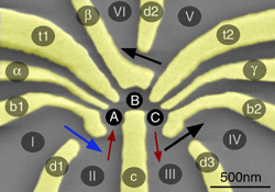
Figure 1. SEM micrograph of the sample structure. Gate electrodes (bright color) are used to electrostatically define a TQD and three QPCs. The approximate position of the QDs are depicted by black circles. Arrows mark possible tunneling current paths through QPCs or the TQD. The blue arrow marks the current path through the QPC used as a charge detector for Fig. 2.
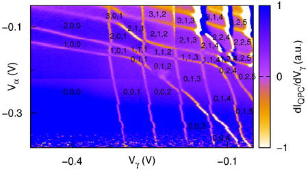
Figure 2.Charge stability diagram of the TQD detected by use of a QPC (blue arrow in Fig. 1). Bright lines of almost horizontal, diagonal and vertical slope depict changes of the electron number on quantum dots A, B and C respectively. Triples of numbers NA,NB,NC denote the number of electrons on each dot in areas of stable charge configuration. In the lower left area, the TQD is uncharged.
Freely suspended quantum dots
Clemens Rössler, Jörg P. Kotthaus, and Stefan Ludwig, in collaboration with Max Bichler, Dieter Schuh, and Werner Wegscheider
We employ quantum dots embedded in nanoscale phonon cavities in order to investigate the electron-phonon interaction. Our phonon cavities are nanoscale bridges excavated from an AlGaAs/GaAs heterostructure. The latter contains a two-dimensional electron system (2DES) which is depleted locally by applying a negative voltage to metallic top gates (Fig. 1).
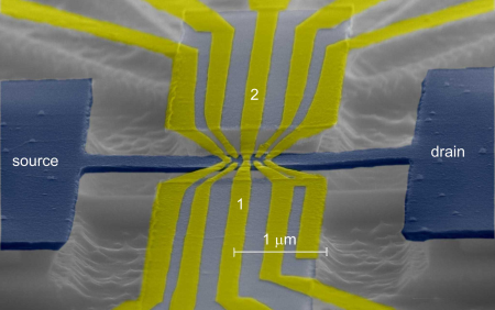
Figure 1.SEM micrograph of a freestanding structure taken under a tilt angle of 85 degrees. Metal gates (yellow) lie on top of the underetched GaAs/AlGaAs heterostructure (blue). Electrons flow between source and drain
By this method it is possible to define 1D-constrictions (i.e. quantum point contacts) or 0D-systems (quantum dots) within the 2DES. Fig. 2 depicts a measurement of our first successfully realised gate defined freely suspended quantum point contact defined by biasing gates 1 and 2 (Fig.1). The differential conductance G decreases quantized in multiples of the fundamental value of G0 = 2e2/h as the one-dimensional subbands are successively depleted.
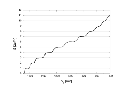
Figure 2. Differential conductance of a quantum point contact on a freestanding bridge as a function of the voltage applied to a pair of Schottky-Gates (see Fig. 1).
Manipulation of the spin of a single electron
Dawid Kupidura , Jörg P. Kotthaus, and Stefan Ludwig, in collaboration with Werner Wegscheider
We aim towards the coherent manipulation of single electrons in double quantum dots laterally defined by surface gates (expanded region in Fig. 1) in GaAs/AlGaAs heterostructures. A strong magnetic bias field parallel to the sample surface serves to allign the magnetic moment of the electron. A much weaker radio frequency magnetic field perpendicular to the sample surface is produced by the integrated loop antenna shown in Fig.1. The sample holder (photograph in Fig. 1) provides impedance matched coupling of the rf-signal between coax-cable and the sample chip. The design aims at spin-resonance experiments on a single electron (ESR). First measurements performed on a single quantum dot show that the rf antenna and sample holder work.
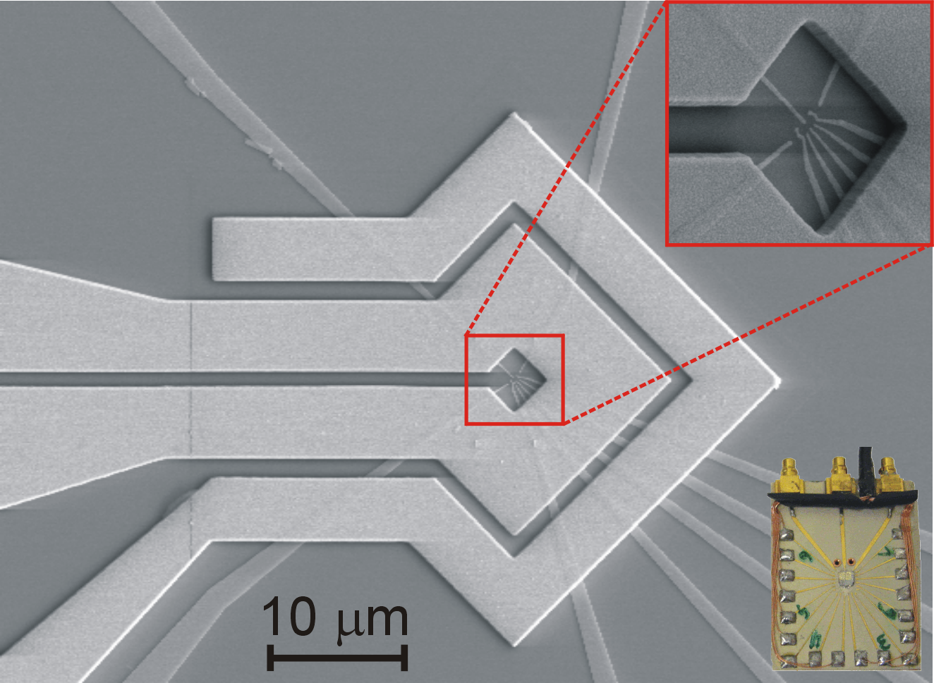
Figure 1. Scanning electron micrograph of the surface of a sample chip showing nanoscale metal top gates defining a double quantum dot (expanded area) covered by a microscale loop antenna. Also shown is a photograph of the sample holder optimized for radio frequency measurements.
Quantum mechanical switching of ballistic electrons
Daniel Harbusch, and Stefan Ludwig, in collaboration with Werner Wegscheider,Tobias Zibold and Peter Vogl
We realized a switchable quantum mechanical beamsplitter for ballistic electrons that could be used as a universal logic gate for quantum computing. The system consists of two coupled, gate defined 1D channels in the 2DEG of a GaAs/AlGaAs heterostructure (Fig. 1a). For appropriate geometric properties of the gate structure, electrons coming from one channel (1) can be switched between two exit channels (3 and 4) by changing the fermi energy of the system e.g. via a back gate. With a gate geometry based on numerical calculations with ³NextNano performed by Tobias Zibold and Peter Vogl we performed first switching experiments on such a device. The results, shown in Fig. 1b are in good agreement with theoretic predictions (Fig. 1c). Strong temperature and magnetic field dependences of the switching effect (not shown) exclude purly classical switching.
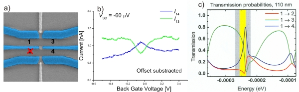
Figure 1. a) A SEM picture of the sample. b) Current transmissions from channel 1 towards channels 3 and 4 measured as a function of the voltage applied to a global gate on the backside of the 0.5 mm thick heterostructrure. Channel 2 is not contacted. c) Transmission probabilities calculated with ³NextNano.
Strain-dependent electrical transport in carbon nanotubes
Christian J.-F. Dupraz, Udo Beierlein, and Jörg P. Kotthaus
Carbon nanotubes are one key building block in nanotechnology, they have gained a tremendous attention in science in the last decade. They show unique material properties: e.g. in mechanics they are known as the stiffest material with an extremely high breaking tension. We combine mechanical manipulation of single wall carbon nanotubes with electrical measurements, to learn how substential strain affects electronic transport. Single wall carbon nanotubes are dispersed on a polyimide film and connected by gold leads. Bending of the substrate exerts strain on the nanotubes and influences the electrical conductance. The bent sections are expected to act as scatterers for the electrons, and hereby the conductance is reduced [1]. The resistance usually increases with larger strain. Some samples show contrary behaviour, with a decrease of resistance followed by a rise (Fig. 1). The findings are in qualitative agreement with theoretical calculations demonstrating a change of the chirality dependent band gap with uniaxial stress [2].
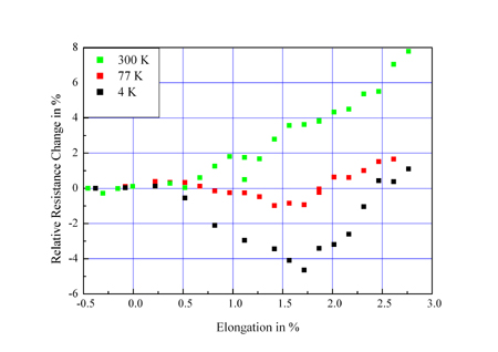
Figure 1. Relative resistance change with strain for a single wall carbon nanotube device at different temperatures.
- Chaplik A.V., JETP Letters 80 (2), 130 (2004).
- Yang L., Anantram M.P, Han J. and Lu J.P., PRB 60 (19), 13874 (1999).
Spatially resolved photoresponse measurements on pentacene thin film transistors
Matthias Fiebig and Jörg P. Kotthaus In collaboration with Martin Göllner, Stefan Schiefer, Bert Nickel, Christoph Erlen, Paolo Lugli
Performance of organic thin film transistors (OTFTs) has improved in recent years dramatically to a degree where devices become suited for widespread applications. Nevertheless electronic properties are still not fully understood. In order to get further insight in electronic transport of these devices we have performed spatially resolved photoresponse measurement with submicron resolution on our bottom contact pentacene TFTs (Fig. 1). We observe inhomogeneous photoresponse due to varying contact quality. This we consider an important limiting factor for electronic transport in bottom contact pentacene transistors (Fig.2). Moreover, the photoresponse is clearly enhanced if the laser beam is focused close to the positively biased electrode. We believe that this is caused by a limited lifetime of the photogenerated electrons that, compared to holes, have a very small mobility in pentacene.
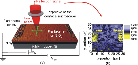
Figure 1. (a) Schematic picture of the focused laser beam on our bottom-contact pentacene TFTs(left). (b) Reflection signal in dependence of the position of the focused laser beam
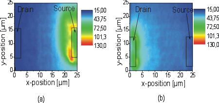
Figure 2. (a) Photoresponse in nA in dependence of the position of the focused laser beam for (a) VSD = -30 V and VG = -30 V and (b) for the exact antisymmetric biasing VSD = +30 V and VG = 0 V. Both maps are equally scaled.
Optics with nanostructures
The optical manipulation of electronic excitations in nano-structures is at the center of our research. To this end, optically generated excitons are studied in various solid state environments. A. Gärtner et al. developed a new method to store long-living excitons in coupled GaAs quantum wells. The excitonic traps are electrostatically controllable und they rely on the quantum confined Stark effect. A. Högele et al. demonstrated how the dispersion and absorption of self assembled InAs and InGaAs quantum dots corresponding to the real and imaginary part of the dielectric susceptibility can be measured by means of a high-resolution laser spectroscopy. Generally, excitons in self-assembled quantum dots constitute an atomic-like solid state system ideally suited to study quantum properties, while it is attractive for realizing qubits. S. Seidl et al. showed how the exciton fine structure in self-assembled quantum dots can be tuned via uniaxial strain. To this end, S. Seidl et al. developed an experimental technique to apply the strain in-situ by a piezo-driven stage. B. Zebli et al. developed a chemical scheme to self-assemble hybrid structures for optoelectronic studies. The hybrid structures are made out of single wall carbon nanotubes, proteins, and nanocrystals.
Storage of long-living excitons in microstructured traps
Andreas Gärtner, Alexander W. Holleitner, and Jörg P. Kotthaus, in collaboration with Dieter Schuh
Trapping and confining long-living excitons attracts much scientific interest especially in the field of Bose-Einstein condensation (BEC) of excitons. The creation of high exciton densities which are suitable for BEC requires efficient trapping techniques. Whereas the motion of excitons can be manipulated in detail [1-3], exciton confinement still remains a challenge. We developed a new method for storing long-living excitons in line-shaped traps (Fig. 1a) [4,5]. The trap for excitons is generated via two metallic surface gates which are in close vicinity (Fig 1b). The semi-transparent gates were micro-structured photo-lithographically on top of a GaAs/AlGaAs structure containing coupled quantum wells. Both surface gates differ by the presence/absence of a SiO2 layer which is sandwiched between the gate and the semiconductor. A line-shaped in-plane harmonic trap for excitons is formed along the interface of both gates. The trap can be switched “off” and “on” electrically via the gate voltages. The measured trapping potential is approximated by a harmonic function with spring constants of about k = 11 keV/cm2 [4,5].
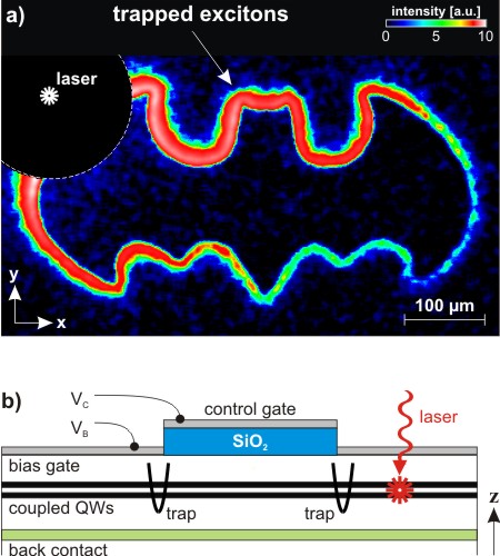
Figure 1. (a) Arbritarily shaped trap for laser-generated excitons (the exciton photoluminescence is color-coded). (b) Cross section of the sample. The trap is realized at the interface of two adjacent top gates at voltages VB and VC, respectively and is elongated laterally along the interface.
- A. Gärtner et al., Physica E 32, 195 (2006).
- A. Gärtner et al., Appl. Phys. Lett. 89, 052108 (2006).
- J. P. Kotthaus, Phys. stat. sol (b) 243, 3754 (2006).
- A. Gärtner et al. (in preparation).
- A. Gärtner, PhD thesis (2006).
Absorptive and dispersive optical responses of excitons in a single quantum dot
Alexander Högele, Martin Kroner,Stefan Seidl, and Khaled Karrai in collaboration with B. Alén, R. J. Warburton, A. Badolato, G. Medeiros-Ribeiro and P. M. Petroff
The dielectric susceptibility of a single quantum dot was determined experimentally. Both the dispersion and absorption of self assembled InAs and InGaAs quantum dots corresponding to the real and imaginary part of the dielectric susceptibility were measured with high-resolution laser spectroscopy in a Fabry-Perot setup at 4.2 K. In this experiment, the weak electromagnetic fields scattered by the excitonic transitions in the quantum dot are made to interfere with the reference laser excitation field [1].
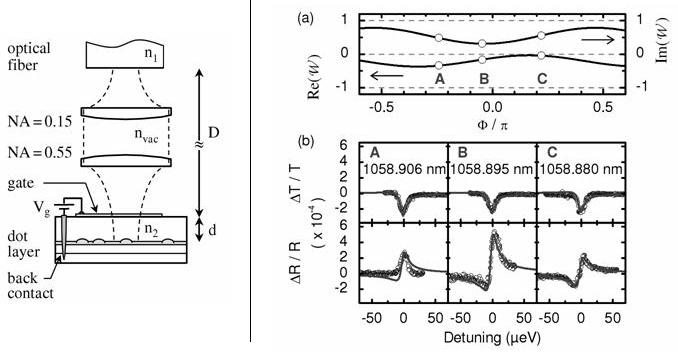
Figure 1. (Left) To interfere the quantum dot light with the reference laser a confocal cavity with length D = 10 mm was defined by the samples surface and polished end of an optical fiber. The dots are placed 150 nm below the surface. (Right) (a) Absorptive and dispersive weighting function plotted against phase Φ ( adjusted by the cavity length) in units of π. The letters A, B and C mark the phase of the corresponding differential transmission and reflectivity spectra shown in (b) as a function of the detuning. Solid lines in (b) are fits to the data (open circles) according to the model described in [1].
- B. Alén, et al., Appl. Phys. Lett. 89, 123124 (2006).
Effect of uniaxial stress on excitons in a self-assembled quantum dot
Stefan Seidl, Martin Kroner, Alexander Högele, and Khaled Karrai in collaboration with R. J. Warburton, A. Badolato and P. M. Petroff
The biexciton-exciton decay cascade in a neutral quantum dot is a possible source for single polarisation entangled photon pairs. However, the fine structure of the exciton destroys this property. Therefore we investigated the fine structure of the neutral exciton in a single self-assembled InGaAs quantum dot under the effect of an applied uniaxial stress. The spectrum of the excitonic Rayleigh scattering was measured in reflectivity using high-resolution laser spectroscopy while the sample was exposed to a tunable uniaxial stress along its [110] crystal axis. We show that using this stretching technique, the quantum dot potential is elastically deformable such that the exciton fine structure splitting can be substantially reduced[1].
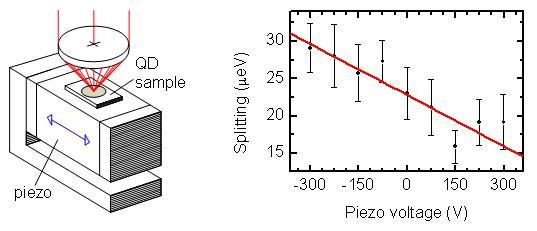
Figure 1. (Left) To control the applied stress in situ, the sample was glued onto a piezo. The fine structure was measured in reflectivity. (Right) The fine structure splitting shows a linear dependence on the applied stress, which is proportional to the piezo voltage.
- S. Seidl, et al., Appl. Phys. Lett. 88, 203113 (2006).
Synthesis of hybrid systems made of single wall carbon nanotubes, nanocrystals and proteins
Bernd Zebli, Markus Mangold, Alexander W. Holleitner, and Jörg P. Kotthaus in collaboration with I. Carmeli, C. Carmeli, S. Richter
In this project, hybrid systems made of individual colloidal nanocrystals, proteins and single wall carbon nanotubes are synthesized via a self-assembly technique, taking advantage of the strong non-covalent biotin-streptavidin-hydrogen bond interaction. To this end, the single wall carbon nanotubes are first functionalized with biotin molecules and then bound to chemically functionalized proteins or nanocrystals which are covered with streptavidin molecules. Individual hybrid systems are adsorbed onto an insulating SiO2 wafer, analyzed by atomic force microscopy, and finally contacted by electrodes using electron beam lithography. The hybrid systems are characterized using optoelectronic charge transport measurements under resonant optical excitation of the constituents of the hybrid nanosystem.
Nanomechanical systems
Nanomechanical systems are realized by lithographic techniques that are capable to create freestanding objects in silicon and other materials, with thickness and lateral dimensions down to about some 10 nanometers. Shrinking mechanical devices in thickness, width and length leads to reduced mass, increased resonant frequency, and lowered force constants of these systems. Therefore nanomechanical systems are both fascinating objects for fundamental studies in the quantum regime and promising for a large variety of applications such as extremely sensitive sensors and actuators. Advances in the field include improvements in fabrication processes, new methods for actuating and detecting motion at the nanoscale. A still challenging problem is how to easily excite nanomechanical elements and control their motion. In both areas we achieved substantial progress.
Fabrication and characterization of nanomechanical resonators for coupling to Bose-Einstein condensates
Stephan Camerer, Daniel R. König, and Jörg P. Kotthaus in collaboration with Theodor W. Hänsch, Jakob Reichel, Philipp Treutlein
Object of this work is the coupling of Bose-Einstein condensed atoms to a nanomechanical resonator (Figure1). By optimizing the fabrication process freely suspended nanosturctures with magnetic islands on top were realized (Figure2). The mechanical characteristics were determined by studying the Brownian motion of the cantilevers. The measured quality factor is in the range between 2000 and 3000 and the resonance frequency around 500 kHz. The magnetic structures were characterized by scanning force spectroscopy. The magnetic trap for the Bose-Einstein can be generated by a current through 1 µm thick gold wires.
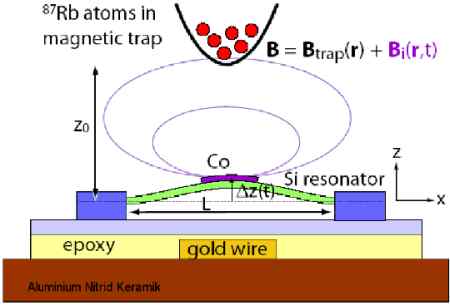
Figure 1. A moving nanomechanical silicon resonator with a ferromagnetic island on top creates a fluctuating magnetic field at the position of a Bose-Einstein condensate, which is captured in a magnetic trap. The trap is induced by the current through the gold wires on the the chip.
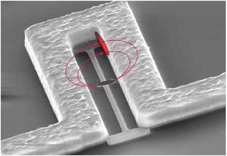
Figure 2.In between the omega-shaped gold wire a freely suspended double clamped nanomechanical resonator with a ferromagnetic island is placed. The movement of the resonator couples to the sketched Bose-Einstein condensate by the fluctuations of the magnetic field.
Optical cooling of a micro-mirror of wavelength size
Ivan Favero, Constanze Metzger, Stephan Camerer, Daniel R. König, Heribert Lorenz, Jörg P. Kotthaus, and Khaled Karrai
We investigated the passive optical cooling of the Brownian motion of a cantilever suspended micromirror (Fig. 1a, 1b). We show that laser cooling is possible for a mirror of size in the range of the diffraction limit (at λ = 1.3 µm) (Fig. 2). This represents the tiniest mirror optically cooled so far, with a mass of 11.3 pg, more than 4 orders of magnitude lighter than current mirrors used in cavity cooling. The reciprocal effect of cooling is also investigated and opens the way to the optical excitation of MHz vibrational modes under continuous wave laser illumination [1].
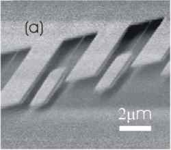
Figure 1. SEM picture of the paddle micro-mirrors.
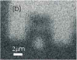
Figure 2. Cavity in situ optical imaging of one micro-mirror.
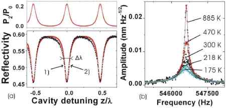
Figure 3. (a) Bottom: Measured (squares) and modeled (circles) reflectivity of the cavity. Top: Simulated ratio of the light power sent on the cavity which impinges on the mirror-paddle M2. (b) Brownian motion amplitude spectra at low laser power P1 (squares labeled 300K) and at higher laser power for negative detuning 1 (circles labeled 218K and 175K respectively for P2 and P3) and positive detuning 2 (triangles labeled respectively 470K and 885K for P2 and P3).
- Favero I., Metzger C., Camerer S., König D.R., Lorenz H., Kotthaus J.P., Karrai K. Appl. Phys. Lett. 90, 104101, 2007
Nanomechanical resonators under high tensile stress
Quirin Unterreithmeier, Daniel R. König, and Jörg P. Kotthaus
The motion of nanostrings under high tensile stress (1.2 GPa) is found to have a Q-factor up to 200000 (low internal damping) at room temperature [1]. Often sensitivity scales with the Q-factor. We study the effect of tunable tensile stress on frequency and Q-factor. The resonators are fabricated using standard top down lithography and subsequent RIE- and wet-etching methods (Fig. 1). Resonators made from silicon nitride were processed, with lengths ranging from 13 to 40µm. width and height are 200 nm. The resonators are driven using a piezo actuator. A static tensile stress of 1.4 GPa resulting from the LPCVD process during wafer fabrication leads to high Q-factors (Fig. 2).
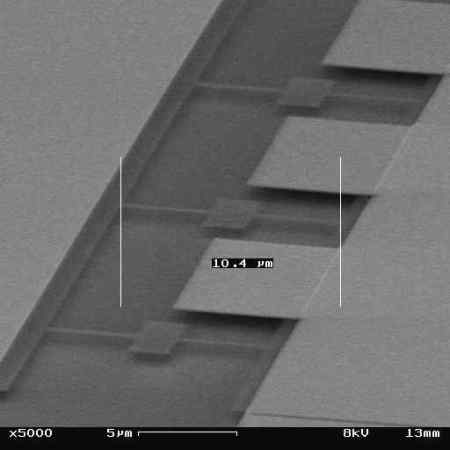
Figure 1. SEM picture of some fabricated cantilevers.
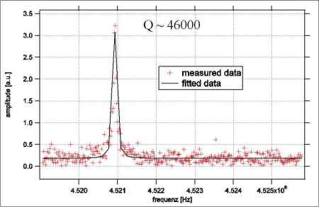
Figure 2.Fitting the resulting spectra with a lorentian function yields the eigenfrequency and Q-factor.
- Verbridge S. et al., J. Appl. Phys. 99, 124304 (2006)
Excitation of micro- and nano-pillars
Philipp Paulitschke, and Heribert Lorenz in collaboration with Achim Wixforth
We succeeded in fabricating large arrays of micro- and nano-pillars by conventional optical and electron beam lithography followed by RIE-etching or wet chemical etching (Fig. 1). The samples are excited by piezo transducers [1] or by surface acoustic waves. They are investigated in an interferometric set-up as well as in the SEM (Fig. 2). The high aspect ratio pillars show eigenfrequencies of the fist harmonic mode ranging from 100 kHz up to 10 MHz with quality factors of about 2000-3000 (Fig. 3). The measured eigenfreqencies and the simulations are in good agreement.
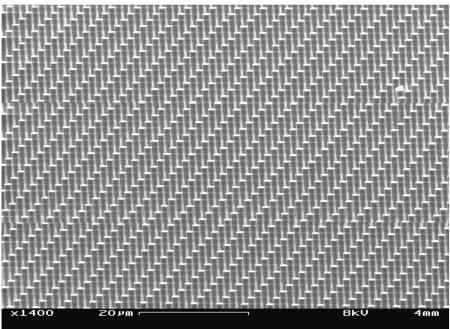
Figure 1. SEM picture of a mirco-/nanopillar array.
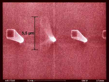
Figure 2. SEM picture of a micro-/nanopillar in motion.
Figure 3. Fitting the resulting spectra yields the eigenfrequency and Q-factor
- Jänchen G., Hoffmann P., Kriele A., Lorenz H., Kulik A.J., Dietler G. Appl. Phys. Lett. 80, 4623, 2002
Nanobioscience
Surface-bound DNA-based nanodevices driven by chemical oscillations
Tim Liedl, Michael Olapinski, and Friedrich C. Simmel
Artificially constructed DNA-based nanodevices can cyclically undergo large conformational changes in response to the presence of certain trigger molecules such as other DNA strands or to changes of the environmental conditions. So far, in most cases DNA-based devices have been controlled by an external operator, who added the effector DNA strands or changed the buffer conditions manually. As an approach towards autonomous motion of molecular machines, our group had previously demonstrated a pH-dependent DNA switch in solution, which reacted on the pH changes of a chemical oscillator run in a semibatch reactor [1]. By attaching the pH-dependent DNA switch to a solid substrate an run the pH oscillator in a continuously stirred tank reactor (CSTR), we were recently able to overcome an essential drawback of the semibatch setup - the damping of the oscillations - and achieve continuous opening and closing of the surface-bound DNA switch over many undamped oscillations [2].
- T. Liedl and F.C. Simmel, Nano Letters 5, 1894-1898 (2005).
- . T. Liedl, M. Olapinski, F. C. Simmel, Angew. Chem. Int. Ed. 45, 5007-5010 (2006).
A DNA signal translator
Stefan Beyer, and Friedrich C. Simmel
DNA-based nanotechnology provides the possibility to combine simple information processing tasks with mechanical or chemical action. An example for such a combination is the thrombin aptamer, which binds to the protein "thrombin" in a sequence-specific manner. The addition of a DNA strand complementary to the sequence of the aptamer can induce the release of the protein by a conformational change of the aptamer strand [1]. In order to uncouple the input sequence from the sequence needed for protein release we designed and successfully employed a signal translator based on branch migration and the action of the endonuclease FokI [2]. For future applications the input strand could be derived from disease related DNA sequences, which then would trigger the release of a therapeutic protein.
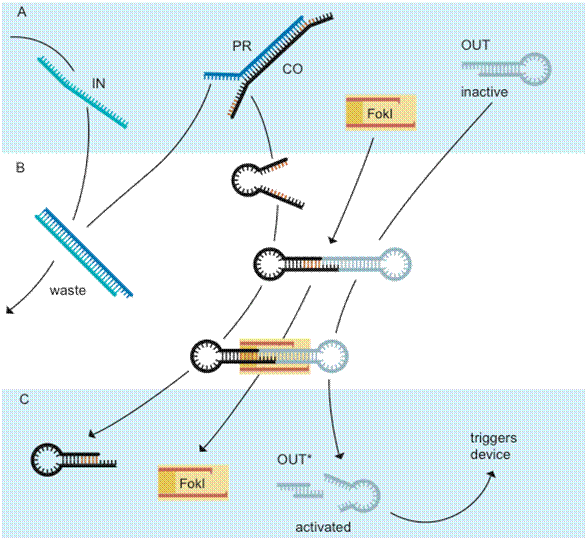
- W. U. Dittmer, A. Reuter, and F. C. Simmel, Angew. Chem Int. Ed. 43, 3550-3553 (2004).
- S. Beyer and F. C. Simmel, Nucleic Acids Research 34, 1581-1587 (2006).
Single molecule characterization of DNA tweezers
Barbara Müller, Andreas Reuter, Friedrich C. Simmel, and Don Lamb
Single molecule studies of biological molecular machines reveal many interesting features which are usually missed in bulk experiments. Bulk experiments characterize the average behavior of a large number of molecules, whereas single molecule studies also provide information on individual properties. In a CeNS-collaboration with Don Lamb and Barbara Müller from the LMU chemistry department, we recently used single-pair fluorescence resonance energy transfer (spFRET) experiments to study one of the prototype DNA-based molecular machines - the [1]. In spFRET experiments, the energy transfer between fluorophores is measured on a single molecule level and the results are evaluated statistically. FRET provides information on the distance between two fluorophores and can therefore be used to study the conformation of biomolecules. In contrast to earlier bulk experiments, spFRET characterization of DNA tweezers revealed the presence of subpopulations which can be attributed to incorrectly assembled molecular devices. It is expected that single molecule techniques will become increasingly important for the future development of more complex artificial molecular machines.
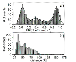
- B. Müller, A. Reuter, F. C. Simmel, and D. C. Lamb, "Single-pair FRET characterization of DNA tweezers", Nano Letters 6, 2814-2820 (2006).
Membranes and ion channels in high-frequency electrical fields
Michael Olapinski, Niels Fertig, and Friedrich C. Simmel
Many biological molecules and structures exhibit large dipolar moments and are strongly influenced by electrical fields. In particular in bilayer membranes and ion channels, electrical fields contribute actively to their biological function. In a cooperation with Nanion Technologies GmbH, we investigate the interaction between external electrical fields of frequencies extending to the Gigahertz range and bilayer or cell membranes containing pore forming peptides or ion channels, in order to examine the dynamic behavior of these systems and to identify methods to externally control their biological function. We recently succeeded in the detection of supported lipid bilayer formation and subsequent incorporation of pore forming Alamethicin peptides in the Gigahertz transmission signal of a lithographically defined coplanar waveguide [1]. In another approach, whole cell currents under the influence of high-frequency (HF) irradiation are investigated, using a planar patch-clamp setup, pulsed HF and lock-in demodulation of the current variations. One major challenge is the discrimination of the thermal influence of HF electrical fields from specific dipolar effects on ion channels. We are currently studying the effects with different pulse modulation frequencies (see fig. 1, manuscript in preparation).
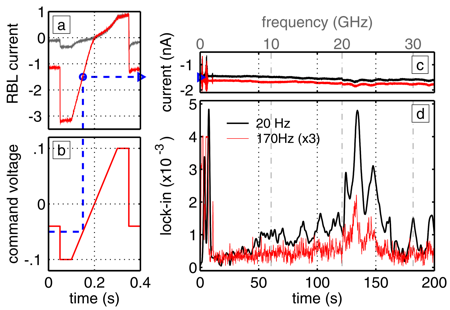
Figure 1. RBL cells, incorporating an inward rectifying potassium channel are kept at a negative potential (b, dashed blue line, scale in V) so that a strong inward current is flowing when external potassium is present (a, red; gray: low potassium). Current (c) and lock-in traces (d) are recorded for 200s, while a HF sweep from 10 MHz to 33 GHz is applied. The lock-in signal represents the relative current variation (displayed for two modulation frequecies in d).
- Olapinski M., Manus S., George M., Brüggemann A., Fertig N. and Simmel F. C., “Detection of lipid bilayer and peptide pore formation at gigahertz frequencies”, Appl. Phys. Lett. 88, 013902 (2006).
Diploma theses completed in 2006
- Stephan Camerer
"Fabrikation und Charakterisierung eines nanomechanischen Systems zur Ankopplung an ein Bose-Einstein Kondensat" - Alexander Ortlieb
"Laserkühlung nanomechanischer Resonatoren" - Xaver Vögele
"Detektion heißer ballistischer Elektronen mit Quantenpunktkontakten und Fokussierung"
PhD theses completed in 2006
- Stefan Beyer
"DNA-based Molecular Templates and Devices" - Andreas Oliver Gärtner
"Dynamik von Exzitonen in elektrostatisch definierten Potentiallandschaften" - Markus Vogel
"Hochauflösende Ladungsdetektion in Nanostrukturen und an dielektrischen Grenzflächen bei tiefen Temperaturen"
Guest scientists in 2006
- Professor Dr. Valeri Dolgopolov,
Russian Academy of Sciences, Chernogolovka, Russia, Alexander von Humboldt Stiftung - Professor Dr. Mansour Shayegan,
Princeton University, USA, Alexander von Humboldt Stiftung - Professor Dr. Richard Warburton,
Heriot-Watt University, Edinburgh, United Kingdom, SFB 631 - Dr. Vadim Khrapay,
Russian Academy of Sciences, Chernogolovka, Russia, Alexander von Humboldt Stiftung - Dr. Ivan Favero,
Ecole Normale Supérieure, Paris Cedex, France, Alexander von Humboldt Sitftung - Louis Gaudreau,
Université de Sherbrooke, Department de Physique, Quebec, Canada - Dr. Andrew Greentree,
Unitersity of Melbourne, Centre for Quantum Computer Technology, Australia - Prof. Alexander V. Chaplik,
Institute of Semiconductor Physics, Novosibirsk, Russia, Alexander von Humboldt Stiftung - Dr. Julien Gabelli,
Ecole Normale Supèrieure, Paris Cedex, France, Alexander von Humboldt Stiftung - Chia-Ling Chung,
Technische Universität Dresden, Biotechnologisches Zentrum
Group members in 2006
Senior scientists
- Prof. Jörg P. Kotthaus
- Prof. Khaled Karraï
- Prof. Alexander Holleitner
- Dr. Heribert Lorenz
- Dr. Stefan Ludwig
- Dr. Friedrich Simmel
- Dr. Joel Moser
Secretary
- Martina Jüttner
Technical staff
- Hans-Peter Kiermaier
- Wolfgang Kurpas
- Stephan Manus
- Alexander Paul
- Stefan Schöffberger
Ph.D. students
- Stefan Beyer
- Christian Dupraz
- Matthias Fiebig
- Eike Friedrichs
- Andreas Gärtner
- Alexander Högele
- Constanze Metzger (nee Höhberger)
- Klaus-Dieter Hof
- Daniel König
- Martin Kroner
- Dawid Kupidura
- Tim Liedl
- Simone Lingitz
- Michael Olapinski
- Andreas Reuter
- Clemens Rössler
- Stefan Seidl
- Thomas Sobey
- Daniel Schröer
- Xaver Vögele
- Bernd Zebli
Diploma students
- Benjamin Biedermann
- Stephan Camerer
- Daniel Harbusch
- Bernhard Heindl
- Martin Herz
- José Horas
- Lisa Kreuzer
- Alexander Ortlieb
- Philip Paulitschke
- Leo Prechtel
- Stephan Renner
- Georg Schinner
- Quirin Unterreithmeier
- Xaver Vögele
Publications in 2006
- Michael Olapinski, Stephan Manus, Michael George, Andrea
Brüggemann,
Niels Fertig, and Friedrich Simmel
„Detection of lipid bilayer and peptide pore formation at gigahertz frequencies“
Appl. Phys. Lett. 88, 013902-1 - -3 (2006) - K. Sritharan, C. J. Strobl, M. F. Schneider, A. Wixforth, and Z.
Guttenberg
"Acoustic mixing at low Reynold’s number"
Appl. Phys. Lett. 88, 054102-1 - -3 (2006) - Stefan Beyer and Friedrich C. Simmel
"A modular DNA signal translator for the controlled release of a protein by an aptamer"
Nucleic Acids Res. 34, 1581–1587 (2006) - Andreas Gärtner, Dieter Schuh, and Jörg P. Kotthaus
"Dynamics of Long-Living Excitons in Tunable Potential Landscapes"
Physica E 32,195 – 198 (2006) - A. Mueller, A. Darga, A. Wixforth
“Surface Acoustic Wave Studies for Chemical and Biological Sensors”
Nanoscale Devices – Fundamentals and Applications, 3-13 (2006) - P. A. Dalgarno, J. McFarlane, B. D. Gerardot, A. Badolato, P. M. Petroff , K. Karrai, and R. J. Warburton
”Decay dynamics of the positively charged exciton in a single charge tunable self-assembled quantum dot”
Appl. Phys. Lett. 89 , 043107-1 - -3 (2006) - Tim Liedl, Michael Olapinski, and Friedrich C. Simmel
“A Surface-Bound DNA Switch Driven by a Chemical Oscillator”
Angew. Chem. Int. Ed. 45, 5007 –5010 (2006) - C. Boedefeld, J. Ebbecke, J. Toivonen, M. Sopanen, H. Lipsanen, and A. Wixforth
”Experimental investigation towards a periodically pumped single-photon source”
Phys. Rev. B 74, 035407-1 - -5 (2006) - A.K. Huettel, S. Ludwig, H. Lorenz, K. Eberl, and J.P. Kotthaus
"Molecular states in a one-electron double quantum dot"
Physica E 34, 488–492 (2006) - A. Gaertner, A. W. Holleitner, D. Schuh, and J. P. Kotthaus "Drift mobility of long-living excitons in coupled GaAs quantum wells" Appl. Phys. Lett. 89, 052108-1 - -3 (2006)
- D. R. Koenig, C. Metzger, S. Camerer, and J. P. Kotthaus
“Non-linear operation of nanomechnical systems combining photothermal excitation and magneto-motive detection”
Nanotechnology 17, 5260-5263 (2006) - B. Alén, A. Hoegele, M. Kroner, S. Seidl, K. Karrai, R. J. Warburton, A. Badolato, G. Medeiros-Ribeiro, and P. M. Petroff
”Absorptive and dispersive optical responses of excitons in a single quantum dot”
Appl. Phys. Lett. 89, 123124-1 - -3 (2006) - V.S. Khrapai, S. Ludwig, J.P. Kotthaus, and W. Wegscheider
"A double-dot quantum ratchet driven by an independently biased quantum point contact"
Phys. Rev. Lett. 97 , 176803-1 - -4 (2006) - A.K. Huettel, S. Ludwig, K. Eberl, and J.P. Kotthaus "Spectroscopy of molecular states in a few-electron double quantum dot" Physica E 35, 278-284 (2006)
- D.M. Schroeer, A.K. Huettel, K. Eberl, S. Ludwig, M.N. Kiselev, and B.L. Altshuler
"Kondo effect in a one-electron double quantum dot: Oscillations of the Kondo current in a weak magnetic field" Phys. Rev. B 74, 233301-1 - -4 (2006) - J.P. Kotthaus
”Manipulating luminescence in semiconductor nanostructures via field-effect-tuneable potentials”
phys. stat. sol. (b) 243, 3754–3763 (2006) - M. Kroner, A. Hoegele, S. Seidl, R. J.Warburton, B. D. Gerardot, A. Badolato, P. M. Petroff, and K. Karrai
"Voltage-Controlled Linewidth of Excitonic Transitions in a Single Self-Assembled Quantum Dot" Physica E 32, 61-64 (2006) - S. Seidl, A. Hoegele, M. Kroner, K. Karrai, A. Badolato, P.M. Petroff, R.J. Warburton
”Tuning the cross-gap transition energy of a quantum dot by uniaxial stress”
Physica E 32, 14-16 (2006) - S. Seidl, M. Kroner, A. Hoegele, K. Karrai, R. J. Warburton, A. Badolato, P. M. Petroff
“Effect of uniaxial stress on excitons in a self-assembled quantum dot”
Appl. Phys. Lett. 88, 203113 -1 - -3 (2006) - Mete Atatuere, Jan Dreiser, Antonio Badolato, Alexander Hoegele, Khaled Karrai, Atac Imamoglu
”Quantum-Dot Spin-State Preparation with Near-Unity Fidelity”
Science 312, 551 (2006) - Khaled Karrai
”A cooling light breeze”
News and Views Article in Nature 444, 41 (2006) - B. K. Mueller, A. Reuter, F. C. Simmel, and D. C. Lamb
“Single-Pair FRET Characterization of DNA Tweezers”
Nano Lett. 6, 2814-2820 (2006) - A. Genovesio, T. Liedl, V. Emiliani, W. J. Parak, M. Coppey-Moisan, and J.-C. Olivo-Marin
"Multiple Particle Tracking in 3-D+t Microscopy: Method and Application to the Tracking of Endocytosed Quantum Dots" IEEE Transact. on image processing 15, 1062-1070 (2006) - A.W. Holleitner, V. Sih, R. C. Myers, A. C. Gossard, and D. D. Awschalom
"Suppression of Spin Relaxation in Submicron InGaAs Wires" Phys. Rev. Lett. 97, 036805 -1 - -4 (2006) - H. Knotz, A. W. Holleitner, J. Stephens, R. C. Myers, and D. D. Awschalom
"Spatial imaging and mechanical control of spin coherence in strained GaAs epilayers" Appl. Phys. Lett. 88, 241918 -1 - -3 (2006) - F. W. Beil, R. H. Blick, A. Wixforth, W. Wegscheider, D. Schuh and M. Bichler
“Observation of single-defect relaxation in a freely suspended nano resonator“
Europhys. Lett., 76, 1207–1213 (2006)
Invited talks in 2006
Jörg P. Kotthaus
- " Electron Transport via Suspended Nanosystems" International Conference on Nanoscience and Technology, ICN+T 2006, Basel, Switzerland July 30 – August 04, 2006
Alexander Holleitner
- "Spin relaxation in InGaAs wires: Transition from 2D to 1D" Conference "6th Rencontres du Vietnam" Hanoi, Vietnam August 06-12, 2006
- "Spin relaxation in InGaAs Wires: Transition from 2D to 1D" International workshop on "Solid State based Quantum Information Processing", Herrsching, Germany Mai 26, 2006
Stefan Ludwig
- "A Double Dot Quantum Ratchet Driven by a Nearby Quantum Point Contact" International Workshop on Solid State Based Quantum Information Processing, Herrsching, Germany May 24 - 26, 2006
- "Wechselwirkende Elektronen in fast leeren Quantenpunkten " Rundgespräch: Elektronische Struktur von Festkörpern, Experiment und Theorie, Bad Honnef, Germany March 1-3, 2006
Friedrich Simmel
- "Molecular information processing and DNA nanodevices " DNA 12, 12th International DNA computing meeting, Seoul June 2006
- "Driving biomolecular nanodevices with chemical oscillators" Gordon Research Conference on "Chemical oscillations and dynamical instabilities in chemical systems", Oxford July - August 2006
- "DNA nanodevices and DNA self-assembly" International Workshop on Self-assembly of Complex Nanostructures, FAHL-Academia, Leipzig September 2006
- "DNA nanodevices and DNA self-assembly" DFG-JST joint workshop on nanoelectronics, Tokyo November 2006
- "Functional DNA nanodevices " Nanomec 06 Symposium, Bari November 2006
Stefan Seidl
- " Modulating the optical response of a quantum dot with a voltage" 2nd International Workshop on Modulation Spectroscopy of Semiconductor Structures (MS3), Wroclaw, Poland June 30, 2006
Senior scientists of cooperating groups
- Gerhard Abstreiter, Max Bichler, Dieter Schuh
Walter Schottky Institut, TU München, Germany. - S. James Allen
University of California, Santa Barbara, USA. - Boris Altshuler
Columbia University, New York, USA. - David Awschalom
University of California, Santa Barbara, USA. - Thomas Bein
CeNS, LMU Munich, Germany. - Robert Blick
University of Wisconsin-Madison, USA. - Alik Chaplik
Institute of Semiconductor Physics, Novosibirsk, Russia. - Valeri Dolgopolov
Russian Academy of Sciences, Chernogolovka, Russia. - Karl Eberl
Max-Planck-Institut für Festkörperforschung, Stuttgart, Germany. - Jochen Feldmann
CeNS, LMU München, Germany. - Niels Fertig
Nanion GmbH, München, Germany. - Jorge M. Garcia
Instituto de Microelectronica de Madrid, Spain. - Hermann Gaub
CeNS, LMU Munich, Germany. - Arthur C. Gossard
Materials Department, University of California - Santa Barbara, USA. - Alexander O. Govorov
Institute of Semiconductor Physics, Novosibirsk, Russia, and Ohio University, USA - Theodor W. Hänsch
LMU Munich, Germany. - Wolfgang Heckl
CeNS, LMU Munich, Germany. - Atac Imamoglu
Department of Physics, ETH Swiss Federal Institute of Technology, Zurich - Karl-Heinz Kunzelmann
Dental Science, LMU, Munich - Don Lamb
CeNS, LMU Munich, Germany. - Paul Leiderer
University of Konstanz, Germany. - Axel Lorke
Universität Duisburg-Essen, Germany. - Wolfgang Parak
CeNS, LMU Munich, Germany. - Pierre M. Petroff
University of California - Santa Barbara, USA. - Joachim Rädler, Bert Nickel
LMU München, Germany. - Mansour Shayegan
Princeton University, USA. - Ulrich Schubert
Eindhoven University of Technology, Dutch Polymer Institute, Eindhoven, Netherlands. - Jan von Delft
CeNS, LMU Munich, Germany. - Richard Warburton
Heriot-Watt University, Edinburgh, U.K. - Werner Wegscheider, Christoph Strunk
Institut für Angewandte und Experimentelle Physik, Universität Regensburg, Germany. - Andreas Wieck
Ruhr-Universität Bochum, Germany. - Achim Wixforth
Universität Augsburg, Germany.
Financial support in 2006
Funding of this work via the following agencies is gratefully acknowledged: