

Research report 2000
Preface
This is our 7th web-based research report since we went 'online' in 1994. Since then, our website has attracted a lot of attention from all over the world and meanwhile serves as an information source not only for our physics colleagues and interested students but also for those out there, who simply want to know on which subjects their 'tax Euros' are working. We appreciate the tremendous activity on our server and do encourage everybody to come by and stay for a while!
For our group, the last year was an extremely sucessful one:
In total, the group published 35 scientific papers, and presented 26 invited talks on international conferences and workshops on various subjects and most importantly, 7 students finished their Diploma or PhD thesis. Dr. Richard Warburton accepted a professorship at the University of Edinburgh and Dr. Axel Lorke went as a professor to the University of Duisburg - we wish them all the best! Many visitors from abroad choose to spend some time with us or came by to give seminar talks.
Finally, we would like to encourage the readers of this (although somewhat delayed) report to contact us and to share their comments and ideas with us.....
Overview
Modern semiconductor technology nowadays combines more than ten million different transistors on a single chip barely as big as a thumbnail to form an extraordinary complex and sophisticated circuit. Following Moore's law, this very large scale integration will proceed over roughly the next ten years until a single element on a chip will be scaled down to less than about 50 nm. This typical dimension of a single device, however, represents a barrier, beyond which the basic operation of an electronic device starts to be based on fundamentally different mechanisms as compared to the conventional ones.
In a classical silicon MOSFET, for example, the principle of operation is based upon the statistical motion of about 10'000 electrons per square micron, whose number may be varied by an external electrode via electric fields. This movement takes place close to the relatively rough silicon/silicon dioxide interface and is described by diffusive processes, similar to the Brown's motion of molecules.
If, however, the dimension of a device becomes comparable or even smaller than the typical distance between two scattering events, the electrons start to move ballistically, like the balls on a billiard table. Moreover, at these small sizes, the number of electrons within a single device starts to approach one. For even smaller devices, their size becomes comparable to the wavelength of the electrons themselves - typically some ten nanometers in this case: The description of the electrons behaving like little charged spheres starts to fail and to require for a quantum mechanical formulation of the device.
In our group, we investigate the electronic, electrooptical, and electromechanical properties of specially tailored semiconductor structures with typical dimensions of the order or less than 100 nm. Recently, we also started to process and investigate mechanical systems like resonators and oscillators on the nanometer scale. Our goal is the detailed understanding of the new physical phenomena associated with a dramatic reduction of size, to explore new grounds for future device applications, and to be prepared for the day when nano-electronics will take over the role of micro-electronics and Nano-Electro-Mechanic Systems (NEMS) will open new routes to the tiny ultra small universe!
- to boldly go where no person has ever gone before!
The research in our group is based on three fundamental prerequisites:
- Nanotechnology
- Sophisticated electronic and optical experimental techniques
- Quantum mechanical concepts and analysis
Starting from suited semiconductor layered systems, we first have to prepare the desired structures with lateral nanometer size dimensions. We use and develop different nanotechnologies that enable us to scale down the size of our structures to the size of the electronic wavelength. For this purpose, our nanotechnology labs are located in a dust free cleanroom area containing modern semiconductor processing equipment.
As we're always trying to be internationally competitive, we set up a large number of international co-operations with partners being specialized in the epitaxial growth of our high quality starting material. Meanwhile, our nanotechnological techniques are also transferred to different disciplines of leading edge research resulting in newly developed collaborations with highly qualified specialists in x-ray analysis, polymer physics, biophysics and biomedical research.
Secondly, we constantly develop and apply sensitive experimental techniques which enable us to chararcterize and to investigate the electronic and optical properties of our nanometer scale samples over the whole spectral range starting from DC over the microwave and infrared regime, the visible spectrum up to UV. At the same time, we are equipped with facilities allowing fo extremely low temperatures and high magnetic fields - invaluable tools for the detailed understanding of the quantum mechanic phenomena in our devices.
A third prerequisite for our research is a detailed and fundamental theoretical analysis and understanding of nanophysics. Together with many theoretical groups and in a very fruitful atmosphere of collaboration, we try to develop new theories and techniques helping us to understand or to predict the many fascinating effects that we are constantly facing. This is in particular important, as we are not studying systems already existing in nature but try to artificially tailor small pieces of this nature to behave in a desired fashion.
Overview of the different research topics
- Dynamic and Static Lateral Superlattices
-
Electronic Properties of Nanostructures
- Conductance Quantization in an Array of Ballistic Constrictions
- Adiabatic Pumping of Electrons
- On-Chip Spectrometer: Coherent Coupling of two Quantum Dots in an Aharonov-Bohm Geometry
- Quantum Dots for Quantum Computing
- Coherent Superpositions of Double-Dot Molecular States by Microwave Photons
- Single-Crystalline Silicon Lift-Off
- Nano-Electro-Mechanical Systems (NEMS)
- Nanodevices for Interdisciplinary Research
- Optics with Nanostructures
- Statistics
A. Dynamic and Static Lateral Superlattices
- Interaction of Surface Acoustic Waves (SAW) and Low-Dimensional Electron Systems
- Storage of Charge in Voltage Controlled Static Potential Superlattices
Interaction of Surface Acoustic Waves (SAW) and Low-Dimensional Electron Systems
Florian Beil, Peter Halke, Christoph Strobl, Christoph Bödefeld, Sascha Haubrich, Hans-Jörg Kutschera, Martin Streibl, Achim Wixforth, Jörg P. Kotthaus
Surface acoustic waves are modes of elastic energy which can propagate on the surface of different materials. If the substrate is piezoelectric, those waves are accompanied by electric fields which then propagate at the speed of sound. The electric fields of the wave can couple to the mobile carriers within a semiconductor structure and modify its electronic and elastic properties. By measuring the attenuation of the wave and the renormalization of the sound velocity we can, for instance, extract information on the dynamic conductivity of the electron system. We also investigate the possibility to use a SAW for a dynamical lateral potential modulation and we investigate the influence of a SAW onto the optical properties of an electron system. Our experiments presently cover the frequency range between 100 MHz and 6 GHz, corresponding to surface acoustic wavelengths between 30 and 500 nm, respectively.
The SAW - related research in 2000 was again governed by two different topics:
- Hybridization of piezoelectrics and semiconductors, exploring possible device applications and nonlinear effects
- Optical investigations of the SAW - semiconductor interaction
Our recent progress in fabricating high frequency and multi-frequency SAW transducers enables us to expand our SAW transport studies well into the GHz regime. The possibility to generate multiple frequencies on a single device allows for a detailed investigation of the SAW - 2DES interaction as a function of the frequency. On standard semiconductor heterojunctions, however, the strength of this interaction is rather weak. For this reason, we use hybrid structures consisting of a strong piezoelectric (LiNbO3) the active semiconductor layer structure. Here, a thin layer of the semiconductor structure containing the active heterojunction is removed from its substrate and tranferred onto a strongly piezoelectric host substrate.
The SAW - 2DES interaction can be enlarged by two orders of magnitude as compared to the monolithic case. This interaction is now strong enough to become technologically very attractive. Room temperature operation is also possible. Together with the Siemens research lab, we are presently developping new concepts for a technological exploitation of this approach. apart from technologically challenging projects, the hybridization technique also offers nice possibiliteis to explore the interaction between low-dimensional electron systems and surface acoustic waves with very large amplitudes. Here, we focussed on the investigation of nonlinear effects that arise under these conditions. For example, we could show that this nonlinear interaction leads to a strong decrease of the electronic absorption that is linked to a separation of a formally homogenous carrier density in the electronic system into well separated stripes riding the wave.
Our major activities, however, concentrated on the investiagtion of the influence of a SAW on the optical properties of a semiconductor quantum well. Here, we opened a completely new and exciting area of research and attracted a tremendous national and international interest. We observe a strong influence of the SAW on the optical properties of a quantum well . The photoluminescence of the quantum well can be completely quenched under the influence of the SAW. Moreover, we show that the SAW can act as a "Photon Conveyor Belt", where optical signals can be stored by the SAW in the semiconductor and may be re-assembled into light after very long delay times and at a remote location of the sample!
Also, the possibility to deliberately pump a self-assembled quantum dot on the surface of a semiconductor quantum well has been investigated both experimentally as well as theoretically. In collaboration with the group of Prof. Fritz Haake (University of Essen), we have proposed a novel scheme for the generation of a single photon source using surface acoustic waves. A non-classical light might evolve from these studies, that we have also started to perform experimentally.
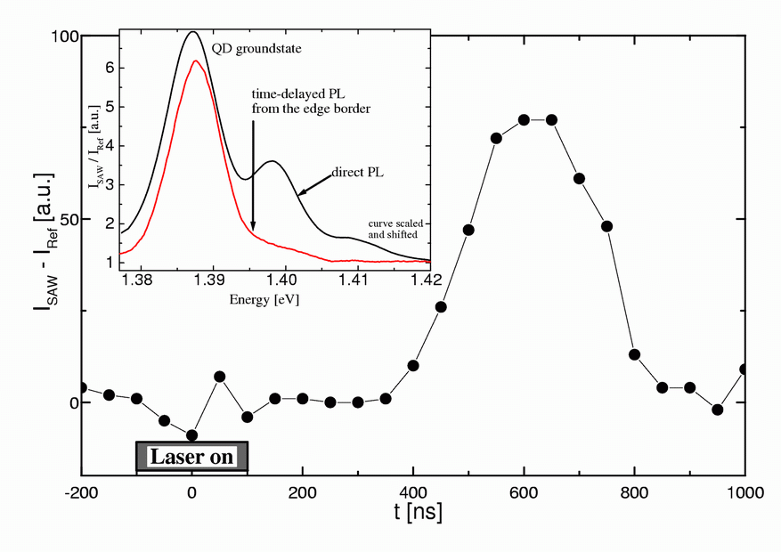
Figure 1. In the main figure the time trace of a photomultiplier is shown. After the transport time of about 500ns a steep rise in the signal is recorded, which results from the light being emitted from the quantum dots. The delay and the duration of the signal can be explained in terms of transport distance and SAW pulse length. In the inset a spectral analysis of this photoluminescence is shown. It clearly corresponds to the spectrum that is recorded without applying a SAW. These results in combination lucidly show that quantum dots can be efficiently pumped with surface acoustic waves.
SAW-induced lateral potential modulations in hybrid systems could be shown to also act as an effective potential modulation for a quasi two-dimensional electron system under quantum conditions. For small wavelengths, we were able to observe commensurability oscillations in the acoustoelectric effect in such structures. Here, the classical cyclotron diameter equals the wavelength of the SAW, leading to pronounced oscillations in the acoustoelectric voltage across the semiconductor sample.
Storage of Charge in Voltage Controlled Static Lateral Potential Superlattices
Jan Krauß, Achim Wixforth, Jörg P. Kotthaus
A stripe-like potential modulation in a semiconductor structure similar to that of a surface-acoustic wave can also be achieved by using interdigitated metal electrodes on top of the structure. When suitable voltages are applied to these electrodes, there is a strong in-plane potential modulation. In contrast to the traveling wave, this modulation is static. However, it can be switched "on" and "off" locally simply by applying different voltages.
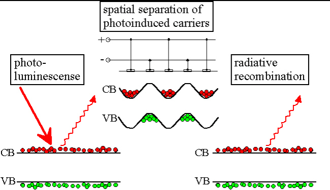
The potential modulation can be used to spatially separate photogenerated electron-hole-pairs, thus increasing carrier lifetime by several orders of magnitudes. When the voltage is removed from the electrodes, the modulation vanishes and the carriers can recombine. This effect can be utilized as a "photonic memory". Up to now, at low temperatures, we achieved storage times of several seconds.
B. Electronic Properties of Nanostructures
- Conductance Quantization in an Array of Ballistic Constrictions
- Adiabatic Pumping of Electrons
- On-Chip Spectrometer: Coherent Coupling of two Quantum Dots in an Aharonov-Bohm Geometry
- Quantum Dots for Quantum Computing
- Coherent Superpositions of Double-Dot Molecular States by Microwave Photons
- Single-Crystalline Silicon Lift-Off
Conductance Quantization in an Array of Ballistic Constrictions
Alida Würtz, Stefan de Haan, Axel Lorke, Jörg P. Kotthaus
We have investigated the transport properties of a two-dimensional array of ballistic constrictions and found that the conductance as a function of gate voltage increases in approximately equally spaced steps. The device was fabricated from a GaAs/AlGaAs-heterostructure with near surface two-dimensional electron gas with typical carrier density of \(6\times10^{11}\,\mathrm{cm}^{-2}\) and mobility of \(8\times10^5\,{\rm cm}^2/{\rm Vs}\). High-resolution electron beam lithography and wet chemical etching techniques have been used to define a lateral superlattice of \(55\times96\) quantum point contacts, i.e. parallel rows of narrow constrictions that are linked every 700 nm. A semitransparent gate, covering the entire structure allows us to vary the electron density and thus the number of occupied one-dimensional subbands in the constrictions.
Fig. 2 shows the gate voltage dependence of the longitudinal conductivity \(\sigma _{xx}\) at two different temperatures.
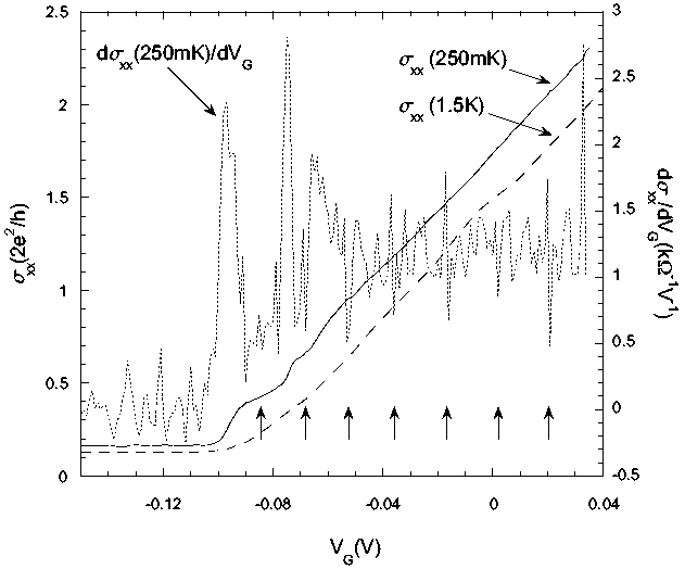
Figure 2. Longitudinal conductivity \(\sigma _{xx}\) at 250 mK (solid line), 1.5 K (dashed line) and derivative \({\rm d}\sigma_{xx}(250\mbox{mK})/{\rm d}V_{G} \propto {\rm d}I/{\rm d}V_{G}\) (dotted line) vs. gate voltage of a lateral superlattice of quantum point contacts. Minima in the differential transconductance, corresponding to plateaus in the conductivity, are indicated by arrows.
Sweeping the gate voltage \(V_{g}\), at sufficiently low temperature (250 mK) both two-terminal and four-terminal measurements of the conductance or resistance reveal a step-like structure of equally spaced plateaus, similar to the characteristics of single [1] or double [2] quantum point contacts. Up to seven oscillations can be identified in the differential transconductance \({\rm d}I/{\rm d}V_{g}\). Our device can therefore be regarded as the realization of a material with a quantized conductance, qualitatively independent of the actual geometry.
The height of the observed conductance steps is not an integer multiple of \(2e^{2}/h\). Surprisingly, it is about three times smaller than this fundamental unit. Thus, this experimental value is neither consistent with the simple model of a mesh of Ohmic resistors, which would lead to a conductivity quantized in units of \(2e^{2}/h\), nor with the picture of coherent transport through a series of quantum point contacts, which would result in an even larger conductance.
A mechanism that could explain our observations is backscattering from the boundaries of the coupled quantum dots formed between the constrictions. In order to find out, how the characteristics of an individual point contact are modified in a large array, we employ a simple model, simulating electronic transport in our structure based on a Landauer-Büttiker-type description. Variing the size of the lattice, it turns out that an addition of quantum point contacts in either of the two dimensions leads to an increase of \(R\), which is in qualitative agreement with the experimental observation.
- B. J. van Wees et al., Phys. Rev. Lett. 60, 848 (1988); D. A. Wharam et al., J. Phys. C 21, L209 (1988).
- D. A. Wharam et al., J. Phys. C 21, L887 (1988); C. G. Smith et al., J. Phys. Condens. Matter 1 , 6763 (1989); M. E. Sherwin et al., Appl. Phys. Lett. 64, 1827 (1994).
Adiabatic Pumping of Electrons
Eva Höhberger, Axel Lorke
Lateral superlattices consisting of two interdigitated but uncentered gates have been used to generate periodic potential modulations in a two-dimensional electron gas (2DEG). Depending on the voltages applied to the gates both symmetric and ratchet-shaped modulations can be defined. Commensurability oscillations in the magnetoresistance which are present in the weakly modulated case can be employed to characterize the resulting potential landscape at the location of the 2DEG. Despite damping and screening of charges this modulation proves to be strongly influenced by the higher harmonics of the gate-induced potential at the surface. This shows that the externally defined symmetry of the superlattice is transferred into the 2DEG with sufficient accuracy.
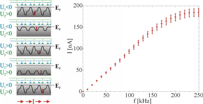
When the gates are periodically biased with rectangular voltage pulses adiabatic pumping of electrons becomes possible when
- the spatial inversion symmetry is broken by the lateral gate structure and
- time inversion symmetry is broken by a temporal phase shift between the voltage pulses applied to the gates.
A dc current is observed which increases linearly with the pumping frequency until saturating at the RC-cut-off frequency. Its direction is defined by the sign of the phase shift between the bias pulses. It reaches its maximum at a pumping amplitude which equals the depletion voltage of the 2DEG.
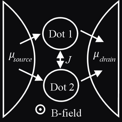
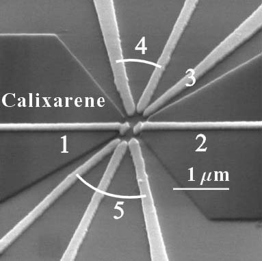
On-Chip Spectrometer: Coherent Coupling of two Quantum Dots in an Aharonov-Bohm Geometry
Alex Holleitner, Robert Blick, Jörg P. Kotthaus
We define two laterally small quantum dots (~15 electrons) in an Aharonov-Bohm geometry in which the coupling between the two dots can be broadly changed. One of the questions which can be considered here, is the entanglement of ferminonic particles, e.g. electrons in a solid state environment. For a system which is depicted in the left figure, it is expected that singlet and triplet states have distinct Aharonov-Bohm-phases [1]. Therefore, this setup is a promising candidate for realizing a quantum bit within a solid state device. In the right figure we present our experimental approach of this concept. On top of a GaAs/AlGaAs heterostructure containing a two dimensional electron gas (2DEG), we evapourate ordinary Schottky gates (numbers 3,4,5) and pattern gates 1 and 2 on an additional resist layer. This 45 nm thick layer is fabricated from Calixarene (hexaacetate p-methycalix[6]arene) with a dielectric constant of about 7. Under appropiate voltage bias the gates not only form two quantum dots in the 2DEG but due to the resist layer provide a two-path quantum dot system as indicated in the left figure. In first experiments we have perfomed transport spectroscopy for different coupling regimes of the two quantum dots. Furthermore, for the first time we extract the magnetic field dependence of the coherent coupling of the two quantum dots [2].
- D. Loss and E.V. Sukhorukov, Phys. Rev. Lett. 84, 1035 (2000).
- A.W. Holleitner, C.R. Decker, K. Eberl, and R.H. Blick, cond-mat #0011044.
Quantum Dots for Quantum Computing
Laura Pescini, Andreas Hüttel, Bert Lorenz, Robert Blick, Jörg P. Kotthaus
Quantum computing in a solid still is a big challenge. One possible approach is the realization of quantum bits with coupled quantum dots. Here we investigate laterally defined quantum dots confined in AlGaAs/GaAs heterostructures comprising a two-dimensional electron gas with extremely high mobility and large phase relaxation length. In order to study decoherence and disspation effects in solids we realize ultra small suspended structures, e.g. nanowires in Silicon-on-Insulator material.
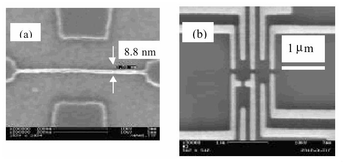
Figure 3. Quantum dots realized in a wire of doped Silicon-on-Insulator material (a) and in a GaAs/AlGaAs-heterostructure (b): Fabrication of Silicon-dots with diameters down to only 15 nm is possible. The large electron density suppresses so far coherent modes to evolve. III/V-heterostructures with multiple Schottky-gates and high mobility two-dimensional electron gases allow the investigation of phase coherence.
Our goal is to study the intricate mechanisms of wave functio interaction in these artificial molecules. We probe the wave function entanglement of coupled quantum dots by applying transport spectroscopy at ultra low temperatures. We determine the strength of this tunnel coupled mode and monitor the magnetic field dependence.
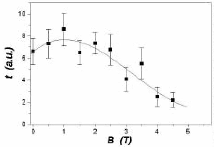
Figure 4. Plotted is the magnitude of the tunnel coupling t. A clear quenching of the coupling with increasing magnetic field is observed. The boxes represent the measured values - the error bars result from the number of crossing points analyzed. The solid line represents a polynomial fit.
Such a coherent mode can be regarded as the essential quantum bit, being the building block of any quantum computational device in a semiconductor (see 15-00) . It still remains to be shown how many operations on these particular qubits are possible and whether it indeed can be integrated with in more complex schemes. In the measurements presented the spin degree of freedom was not yet addressed. We note that the application of II/VI-heterostructures allows the integration of magnetic two-dimensional electrons gases. The further development of this basic research will show if the concepts of quantum computation can be applied successfully on the artificial molecules. In any case this work will lead to a detailed understanding of the fundamental properties of these quantum mechanical systems.
Coherent Superpositions of Double-Dot Molecular States by Microwave Photons
Hua Qin, Robert Blick
A tunnel-coupled double quantum dot is realized from the two-dimensional electron gas (2DEG) of an AlGaAs/GaAs heterostructure by using Schottky gates. Two quantum states (one in each dot) are coupled to form the bonding and anti-bonding molecular states (Fig. 5). The energy difference between the molecular states is well controlled by the relevant gate voltages. The formation of molecular states is observed by both transport and microwave spectroscopy [1]. In transport spectroscopy, tunneling through the bonding state is revealed in the charging diagram. In microwave spectroscopy, photon-assisted tunneling is observed, which stems from the coherent superposition of two molecular states coupled by microwave photons. Such a coherent superposition of two quantum states can be used to realize a quantum bit (qubit)(Fig. 6) [2]. In a single quantum dot, however as we found, a long charge relaxation time is always involved in the coupling between a ground state and an excited state. Hence no qubit can be expected from the ground state and the excited state of a single quantum dot.
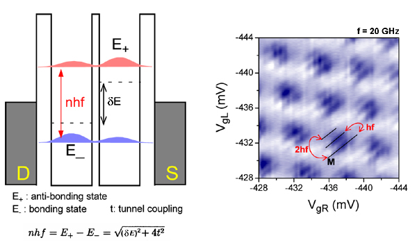
Figure 5. Left: Bonding and anti-bonding molecular states are formed from two hybridized quantum states under a detuning. Right: The bonding and anti-bonding states are coherently coupled by microwave photons, generating sidepeaks beside the main peak (M) in the charging diagram (white: zero current, blue: finite current).
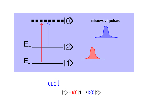
Figure 6. A scheme [2] for realizing a qubit from the superposition of two molecular states by microwave photons.
- H. Qin, A.W. Holleitner, K. Eberl, and R.H. Blick, cond-mat/0011155.
- T. Brandes, F. Renzoni, and R. H. Blick, cond-mat/0104435, to appear in Phys. Rev. B.
Single-Crystalline Silicon Lift-Off
Armin Tilke, Bert Lorenz
We have also developed a technique to mount single-crystalline silicon thin films on arbitrary substrates (see 18-00). We demonstrate in detail the preparation of a 190-nm-thin silicon metal-oxide-semiconductor field-effect transistor (MOSFET) on a silicon-on-insulator film lifted from its substrate and bonded to quartz.
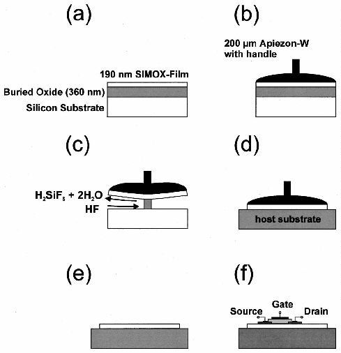
Figure 7. The process of fabricating silicon LO films is shown schematically: Starting from a slightly boron-doped silicon-on-insulator structure (a) the silicon film is covered by a thick Apiezon-W film protecting the surface (b) and subsequently underetched in diluted HF (c) and attached onto an arbitrary substrate by van-der-Waals forces (d). The Apiezon-W is removed (e) and an enhancement MOSFET is defined (f).
Functioning of this hybrid MOSFET on a rigid surface at room temperature is demonstrated.
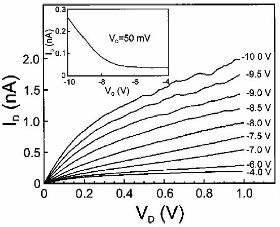
Figure 8. Output characteristic IDvs VD at fixed gate voltages and transfer characteristic [IDvs VG (inset) for the silicon thin-film p-channel LO-MOSFET (T=300 K)].
C. Nano-Electro-Mechanical Systems (NEMS)
- Nano-Mechanical Resonators
- Silicon Nanoelectronics and Nanoelectromechanics
- Electrically Driven Nanotweezers
Nano-Mechanical Resonators
Artur Erbe, Laura Pescini, Dominik Scheible, Robert Blick
Mechanical devices in combination with modern semiconductor electronics offer great advantages as for example their robustness against electrical shocks and ionization due to radiation, which is of great importance for applications in scanning probe microscopy of mechanical cantilevers. Another are of practical applications is found in frequency sources and clocks with microscopical mechanical resonators. The main disadvantage of mechanical devices so far is the low speed of operation. This has been overcome with the realization of nanomechanical resonators, which allow operation at frequencies up to 500 MHz.
In the present work we realized nanomechanical resonators to study its nonlinear dynamics and its mechanical mixing properties. Mixing is of great importance for signal processing in common electronic circuits. Combining signal mixing with the advantages of mechanical systemss is very promising, especially when considering the high speed of operation currently becoming available. Here we present measurements on such a nonlinear nanomechanical resonator, forced into resonance by application of two different but neighboring driving frequencies. In the figure a typical mixing signal is shown in dependence of the magnetic field as a control parameter. This can be modelled on the basis of the Duffing equation, which accurately describes the behavior of the mechanical resonator. The model gives insight into the degree of nonlinearity of the resonator and hence into the generation of higher-harmonic mechanical mixing.
Silicon Nanoelectronics and Nanoelectromechanics
Armin Tilke, Laura Pescini, Bert Lorenz, Robert Blick, Jörg P. Kotthaus
Nowadays single-electron devices are believed to be one of the top-candidates to replace standard Complementary Metal Oxide Silicon (CMOS) transistor technology at the end of the conventional semiconductor roadmap. We investigate the manipulation of electrons in nanostructured semiconductors, especially in silicon with particular emphasis on different realizations of single-electron tunneling devices (see 17-00, 26-00 & 33-00). Silicon-based fabrication technology further allows the use of the manufacturing processes already established in semiconductor industry. Moreover, the use of Silicon-on-Insulator (SOI) films allows the lithographic definition of the currently smallest structure sizes, which are crucial for the room temperature operation of single-electron devices. Lateral structuring of highly doped silicon films allows us to observe quasi-metallic Coulomb-blockade oscillations in shrunken wires where no quantum dot structure is geometrically defined. Embedding quantum dot structures into the inversion channel of a silicon-on-insulator field-effect transistor Coulomb blockade up to 300 K is observed. In contrast to the quasi-metallic structures, in these devices the influence of the quantum mechanical level spacing inside the dot becomes visible.
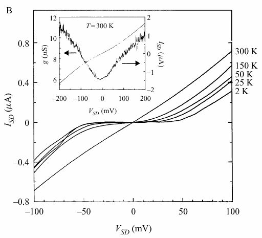
Figure 9. Temperature dependence of the ISD-VSDtrace of an inversion quantum dot at a top gate voltage of \(V_{TG}= 4.5 {\rm V}\). At 300 K clear single-electron effects remain visible.
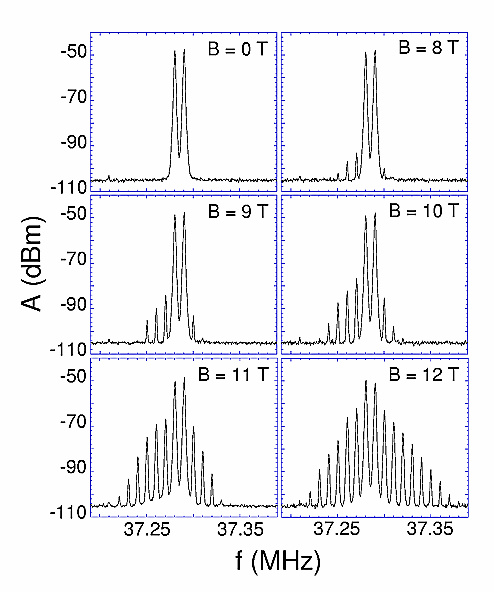
The layer sequence in SOI allows the underetching of these devices in order to realize suspended, highly doped silicon nanostructures. Similar suspended silicon beams are fabricated to form novel nanomechanical resonators that can be excited at radio frequencies up to about 300 MHz. Controlling the vibration frequency by a side-gate voltage, these resonators allow charge detection with a sensitivity of 0.1 e / sqrt(Hz), comparable to that of cryogenic single-electron devices.
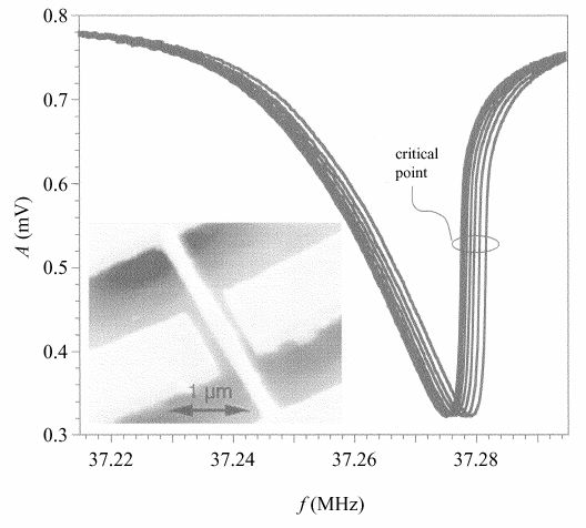
Figure 10. Resonance curves of the reflected rf power of the suspended wire shown in the inset. The resonator is driven into the nonlinear regime by the Lorentz force in a B-field of 12 T applied perpendicularly to the rf current. Different curves are measured at different values of the voltage on one of the sidegates. Inset: SEM micrograph of the structure.
Currently, several technologies are investigated in order to overcome the problems arising from scaling device dimensions down to or even below 10 nm. However, two conditions must be satisfied to successfully integrate single-electron devices in standard technology: Firstly, the devices have to work at room temperature, which requires that their geometrical dimensions are on the order of 5 nm and, secondly, the choice of silicon for fabricating the structures is necessary for compatibility and integrability. Especially silicon-on- insulator (SOI) materials, where a thin film of crystalline silicon is located on top of an insulating layer separating the silicon film from the underlying substrate, are the most promising candidates for such silicon-based SET structures.
Electrically Driven Nanotweezers
Christine Meyer, Bert Lorenz
(see http://www.nano.physik.uni-muenchen.de/~meyer/SFB486TPA2.html)
Motivation and aim of this project is to pick up particles with typical sizes in the range between 10 nm and 100 nm and to release them at a predefined location. Nowadays, the manipulation of nanoparticles is mainly done by atomic force microscopy whereby the result is more stochastically. Our goal is to develop electrically driven nanotweezers, which allow a specific manipulation of nanoparticles.
D. Nanodevices for Interdisciplinary Research
A Planar Chip to Investigate Ion Channels
Niels Fertig, Christine Meyer, Jan Behrends, Robert Blick
Ion channels belong to the basic equipment of every biological cell. Every nerve signal is transduced via ion channels, which makes knowledge about these channels quite important, e.g. for drug screening. The commonly used Patch-clamp-technique is based on a glass pipette, which isolates the channels investigated. If we use a planar chip instead of the pipette, it should be possible to use scanning probe techniques in combination with the current measurements. Presumably the background noise and the time resolution of the current signals measured can also be improved.
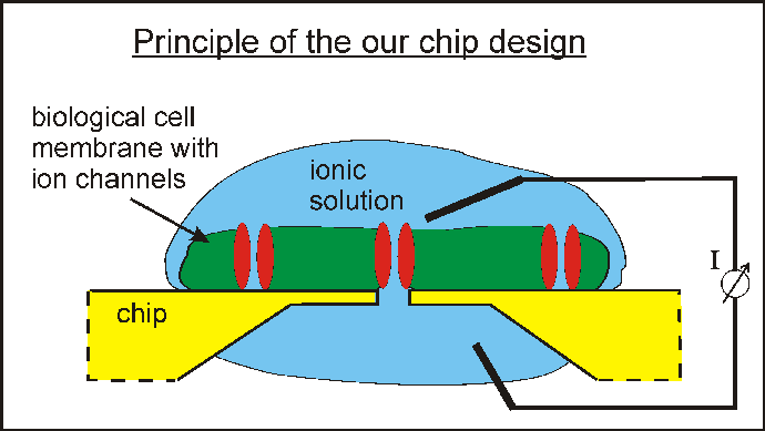
Recently we developed a biochip for monitoring ionic currents through individual ion channels. The chip is based on a quartz or glass substrate, which is microstructured by lithography and different etching techniques.
Recordings from the low weight peptide gramicidin A were taken at extraordinary low background noise levels.
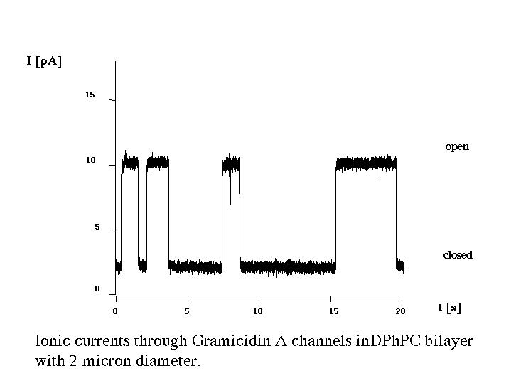
Gramicidin was incoorporated in DPhPC-bilayers and electrical recordings were taken with bandwidth up to 3 kHz. The noise level at this bandwidth was below 300 fA rms.
A report about previous work focusing on similar biochip based on silicon substrates was published in the Applied Physics Letters (2000, Vol. 77, p.1218).
E. Optics with Nanostructures
- Optical Emission from a Charge-Tunable Quantum Ring
- Interfacial Shear Force Microscopy
- Enhanced Reflectivity Contrast in Confocal Solid Immersion Lens Microscopy
Optical Emission from a Charge-Tunable Quantum Ring
Nature, 405, 926
(2000).
R. J. Warburton, C. Schäflein, D. Haft,
F. Bickel, A. Lorke, K. Karraï
Quantum dots or rings are artificial nanometre-sized clusters that confine electrons in all three directions. They can be fabricated in a semiconductor system by embedding an island of low-bandgap material in a sea of material with a higher bandgap. Quantum dots are often referred to as artificial atoms because, when filled sequentially with electrons, the charging energies are pronounced for particular electron numbers; this is analogous to Hund's rules in atomic physics. But semiconductors also have a valence band with strong optical transitions to the conduction band. These transitions are the basis for the application of quantum dots as laser emitters, storage devices and fluorescence markers. Here we report how the optical emission (photoluminescence) of a single quantum ring changes as electrons are added one-by-one. We find that the emission energy changes abruptly whenever an electron is added to the artificial atom, and that the sizes of the jumps reveal a shell structure.
Interfacial Shear Force Microscopy
Phys. Rev. B 62, 13174
(2000).
K. Karraï and Ingo Tiemann
We present an experimental investigation of
lossy and reactive shear forces at the nanometer scale using
quartz-crystal tuning-fork shear-force microscopy. We show
that this technique allows us not only to quantitatively
measure viscous friction and elastic shear stress with a
combination of high spatial and force resolution (better than
10 nm, and less than 1 pN, respectively), but also to obtain
such quantities with the tip positioned at any arbitrary
distance away from direct electrical tunnel contact with the
sample surface. We are proposing that, even under vacuum
conditions, the measured viscous and elastic shear stress
(i.e., velocity dependent) are directly attributable to a
third body filling the tip-sample gap. A simple model is
given that allows us to obtain its local viscosity and shear
modulus as a function of the tip-sample distance, showing
that tuning-fork shear-force microscopy can be applied to
quantitative analysis in nanotribology.
Enhanced Reflectivity Contrast in Confocal Solid Immersion Lens Microscopy
Appl. Phys. Lett. 77,
3459 (2000).
K. Karraï, X. Lorenz
The reflected image of a diffraction limited focused spot is investigated using confocal solid immersion microscopy. We find that the spot's image shows aberrations when reflected off objects with optical indexes lower than that of the solid immersion lens (SIL) material. We demonstrate that such aberrations are only apparent and that the actual size of the spot at the SIL/object interface remains diffraction limited. The aberrations are due to lateral waves at the SIL surface. These von Schmidt waves originate from the total internal reflected components of a diverging spherical wave front. We make use of this image aberration in conjunction with the spatial filtering inherent to confocal microscopy in order to dramatically enhance the optical contrast of objects with low optical indexes.
Statistics
- Diploma Theses completed in 2000
- PhD Theses completed in 2000
- Habilitations completed in 2000
- Guest Scientists, Visitors, and their Sponsors in 2000
- Group Members in 2000
- Publications
- Invited Talks
- Collaborations
- Financial Support
Diploma Theses completed in 2000
- Christine Meyer
Abgabe: 26.07.2000
"Herstellung einer Nano-Patch-Clamp-Sonde aus Quarz" - Thomas Klühspies
Abgabe: 25.08.2000
"Ladungstranport in epitaktische abgelösten zwei-dimensionalen Elektronengasen" - Andreas Kraus
"Getriebene nichtlineare nanomechanische Resonatoren" - Andreas Rathgeber
Abgabe: 15.09.2000
"Manipulation und Transport von Materie in fester und flüssiger Form mittels akustischer Oberflächenwellen"
PhD Theses completed in 2000
- Petra Denk
Koll.: 26.07.2000
"Growth and Electronic Properties of AlAs/GaAs Lateral Superlattices: from 2D to 1D" - Armin Tilke
Koll.: 17.11.2000
"Einzelelektronentransport in Silicon-on-Insulator-Nanostrukturen" - Martin Streibl
Koll.: 18.05.2000
"Statische und dynamische Potentialgitter auf Halbleiterheterostrukturen für optoelektronische Anwendungen"
Habilitations completed in 2000
- Richard Warburton
"Optics of semiconductor nanostructures"
Guest Scientists, Visitors, and their Sponsors in 2000
- Prof. Alik Chaplik
(Inst. of Semiconductor Physics, Novosibirsk, Russia)
SFB 348 - Prof. Valeri Dolgopolov
(Russian Academy of Sciences, Chernogolovka, Russia)
SFB 348 - Dr. Matthew Grayson
(Maryland, USA)
Alexander von Humboldt Foundation - Prof. Dr. Sergio Ulloa
(Ohio University, USA)
Max-Planck Forschungspreis - Dr. A. O. Govorov
(Russian Academy of Sciences, Novosibirsk, Russia)
Volkswagen Stiftung - Dan van der Weide
(Maryland, USA)
Alexander von Humboldt Foundation - Hua Qin
Volkswagen Stiftung, Deutscher Akademischer Austauschdienst
Group Members in 2000
Head of the Group
- Prof. Jörg P. Kotthaus
- Prof. Khaled Karraï
- Dr. Robert Blick
- Dr. Heribert Lorenz
- Dr. Axel Lorke
- Dr. Richard Warburton
- Dr. Achim Wixforth
Secretary
- Eveline Stettner
Technical Staff
- Hans-Peter Kiermaier
- Armin Kriele
- Wolfgang Kurpas
- Stephan Manus
- Klaus Werhahn
Ph.D. Students
- Florian Beil
- Florian Bickel
- Christoph Bödefeld
- Stefan Böhm
- Artur Erbe
- Petra Denk
- Niels Fertig
- Wolfgang Frank
- Stephan de Haan
- Dirk Haft
- Eva Höhberger
- Alexander Holleitner
- Jan Krauß
- Hans-Jörg Kutschera
- Laura Pescini
- Hua Qin
- Christian Schäflein
- Martin Streibl
- Armin Tilke
- Markus Vogel
Diploma Students
- Peter Halke
- Andreas Hörner
- Andreas Hüttel
- Jochen Kirschbaum
- Thomas Klühspies
- Andreas Krauss
- Christine Meyer
- Christina Mooser
- Andreas Rathgeber
- Dominik Scheible
- Christian Schulhauser
- Christoph Strobl
Publications
- 1-00 R.
Blick, A. Erbe, A. Tilke, and A. Wixforth
"Auf dem Weg zur 'Quanten-Mechanik'"
Physikalische Blätter 56, 31-36 (2000) - 2-00 V.
S. Khrapai, E. V. Deviatov, A. A. Shashkin, V. T.
Dologopolov, F. Hastreiter, A. Wixforth, K. L. Campman, and
A. C. Gossard
"Canted Antiferromagnetic Phase in a Double Quantum Well in a Tilted Quantizing Magnetic Field"
Phys. Rev. Lett. 84, 725-728 (2000). - 3-00 A.
W. Holleitner, H. Qin, F. Simmel, B. Irmer, R. H. Blick, J.
P. Kotthaus, A. V. Ustinov, and K. Eberl
"Microwave Spectroscopy on a Double Quantum Dot with an On-Chip Josephson Oscillator"
New Journal of Physics 2, 2.1-2.7 (2000). - 4-00 A.
Lorke, R. J. Luyken, A. O. Govorov, J. P. Kotthaus, J. M.
Garcia, and P. M. Petroff
"Spectroscopy of Nanoscopic Seminconductor Rings"
Phys. Rev. Lett. 84, 2223-2226 (2000). - 5-00 H.
Krömmer, A. Erbe, A. Tilke, S. Manus, and R. H.
Blick
"Nanomechanical Resonators Operating as Charge Detectors in the Nonlinear Regime"
Europhys. Lett. 50, 101-106 (2000). - 6-00 M.
Rotter, W. Ruile, G. Scholl, and A. Wixforth
"Novel Concepts for GaAs/LiNbO3 Layered Systems and their Device Applications"
IEEE, Transaction on Ultrasonics, Ferroelectrics, and Frequency Control 47, 242-248 (2000). - 7-00 M.
Streibl, A. Wixforth, J. P. Kotthaus, C. Kadow, and A. C.
Gossard
"Imaging of Carrier Dynamics in Semiconductor Heterostructures by Surface Acoustic Waves"
Physica E 6, 255-259 (2000). - 8-00 D.
Abush-Magder, F. Simmel, D. A. Wharam, M. A. Kastner, and J.
P. Kotthaus
"Spacing and Width of Coulomb Blockade Peaks in a Silicon Quantum Dot"
Physica E 6, 382-387 (2000). - 9-00 H.
Pettersson, R. J. Warburton, A. Lorke, K. Karraï, J. P.
Kotthaus, J. M. Garcia, and P. M. Petroff
"Excitons in Self-Assembled Quantum Ring-Like Structures"
Physica E 6, 510-513 (2000). - 10-00
R. H. Blick, A. Erbe, H. Krömmer, A. Kraus, and J. P.
Kotthaus
"Charge Detection with Nanomechanical Resonators"
Physica E 6, 821-827 (2000). - 11-00
R. J. Warburton, K. Weilhammer, C. Jabs, J. P. Kotthaus, M.
Thomas, and H. Kroemer
"Collective Effects in Intersubband Transitions"
Physica E 7, 191-199 (2000). - 12-00
R. J. Warburton, C. Schäflein, D. Haft, F. Bickel, A.
Lorke, K. Karraï, J. M. Garcia, W. Schoenfeld, and P. M.
Petroff
"Optical Emission from a Charge-Tunable Quantum Ring"
Nature 405, 926-929 (2000). - 13-00
R. J. Warburton, C. Schäflein, H. Pettersson, D. Haft,
F. Bickel, C. S. Dürr, K. Karraï, J. P. Kotthaus,
G. Rebeiros-Ribeiro, J. Garcia, W. Schoenfeld, J. M. Petroff,
N. Carlsson, W. Seifert, and L. Samuelson
"Interband Optics of Charge-Tunable Quantum Dots"
in "Optical Properties of Semiconductor Nanostructures", Eds. M. L. Sadowski et al. (Kluwer, Dordrecht 2000), pp. 347-363. - 14-00
R. D. Grober, J. Acimovic, J. Schuck, D. Hessman, P. J.
Kindlemann, J. Hespanha, A. S. Morse, K. Karraï, I.
Tiemann, and S. Manus
"Fundamental Limits to Force Detection Using Quartz Tuning Forks"
Review of Scientific Instruments 71, 2776-2780 (2000). - 15-00
R. Blick and H. Lorenz
"Possible Definition of Quantum Bits in Coupled Quantum Dots"
Proceedings of the IEEE International Symposium on Circuits and Systems, May 28-31, 2000, Geneva Switzerland, ISCAS 2000, pp II 245-II 248
#1338.PDF on CD-ROM (ISBB 0-780-5485-0) - 16-00
A. O. Govorov, A. V. Kalameitsev, M. Rotter, A. Wixforth, J.
P. Kotthaus, K.-H. Hoffmann, and N. Botkin
"Nonlinear Acoustoelectric Transport in a Two-Dimensional Electron System"
Phys. Rev. B 62, 2659-2668 (2000). - 17-00
A. Tilke, A. Erbe, L. Pescini, H.
Krömmer, R. H. Blick, H. Lorenz, and J. P. Kotthaus
"Silicon-Based Nanoelectronics and Nanoelectromechanics"
Superlattices and Microstructures 27, 597-601 (2000). - 18-00
A. Tilke, M. Rotter, R. H. Blick, H. Lorenz, and J. P.
Kotthaus
"Single Crystalline Silicon Lift-off Films for MOS-Devices on Arbitrary Substrates"
Appl. Phys. Lett. 77. 558-560 (2000). - 19-00
N. Fertig, A. Tilke, R. H. Blick, J. P. Kotthaus, J. C.
Behrends, and G. ten Bruggencate
"Stable Integration of Isolated Cell Membrane Patches in a Nanomachined Aperture"
Appl Phys. Lett. 77, 1218-1220 (2000). - 20-00
A. Emperador, M. Pi, M. Barranco, and A. Lorke
"Far-Infrared Spectroscopy of Nanoscopic InAs Rings"
Phys. Rev. B 62, 4573-4577 (2000). - 21-00
R. A. Deutschmann, A. Lorke, W. Wegscheider, M. Bichler, and
G. Abstreiter
"Breakdown of Shubnikov-de Haas Oscillations in a Short Period 1D Lateral Superlattice"
Physica E 6, 561-564 (2000). - 22-00
E. V. Deviatov, V. Khaprai, A. A. Shashkin, V. T. Dolgopolov,
F. Hastreiter, A. Wixforth, K. L. Campman, and A. C,
Gossard
"Opening an Energy Gap in an Electron Double Layer System at the Integer Filling Factor in a Tilted Magnetic Field"
JETP Letters 71, 496-499 (2000) - 23-00
P. Denk, M. Hartung, A. Wixforth, K. L. Campmann, A. C.
Gossard
"Depolarization Shift in Coupled Quantum Wells with Tunable Level Spectrum"
Physica E 8, 269-274 (2000). - 24-00
A. Kraus, A. Erbe, and R. H. Blick
"Nanomechanical Vibrating Wire Resonator for Phonon Spectroscopy in Liquid Helium"
Nanotechnology 11, 165-168 (2000). - 25-00
A. Erbe, H. Krömmer, A. Kraus, and R. H. Blick
"Mechanical Properties of Suspended Structures at Radio Frequencies"
Physics B 280, 553-554 (2000). - 26-00
A. Tilke, L. Pescini, R. H. Blick, H. Lorenz, and J. P.
Kotthaus
"Single Electron Tunneling in Silicon Nanostructures"
Appl. Phys. A 71/4, 357-365 (2000). - 27-00
I. Kegel, T. H. Metzger, A. Lorke, J. Peisl, J. Stangl, G.
Bauer, J. M. Garcia, and P. M. Petroff
"Nanometer-Scale Resolution of Strain and Interdiffusion in Self-Assemled InAs/GaAs Quantum Dots"
Phys. Rev. Lett. 85, 1694-1697 (2000). - 28-00
A. Erbe, G. Corso, H. Krömmer, A. Kraus, K. Richter, and
R. H. Blick
"Mechanical Mixing in Nonlinear Nanomechanical Resonators"
Appl. Phys. Lett. 77, 3102-3104 (2000). - 29-00
B. Lorenz
"Nanowelt / Nanoworld"
Form + Zweck 17, 40-52 (2000). - 30-00
K. Karraï and Ingo Tiemann
"Interfacial Shear Force Microscopy"
Phys. Rev. B 62, 13174-13181 (2000). - 31-00
K. Karraï, X. Lorenz, and L. Novotny
"Enhanced Reflectivity Contrast in Confocal Solid Immersion Lens Microscopy"
Appl. Phys. Lett 77, 3459-3461 (2000). - 32-00
S. Böhm, W. J. Parak, M. George, H. E. Gaub, and A.
Lorke
"Characterization of the Field-Effect-Addressable Potentiometric Sensors (FAPS)"
Sensors & Actuators B 68, 266-273 (2000). - 33-00
H. Lorenz, R. H. Blick, A. Tilke, and J. P. Kotthaus
"Manipulation of Electrons in Nanostructures Semiconductors"
Extended Abstract, 4th International Workshop on Quantum Functional Devices, QFD2000, Kanazawa, Japan, 17-20 (2000). - 34-00
R. H. Blick, F. G. Monzon, W. Wegscheider, M. Bichler, F.
Stern, and M. L. Roukes
"Magnetotransport Measurements on Freely Suspended Two-Dimensional Electron Gases"
Phys. Rev. B 62, 17103-17107 (2000). - 35-00
A. Wixforth
"Interaction of Surface Acoustic Waves, Electrons, and Light"
Int. J. High Speed Electronics and Systems 10, 1193-1227 (2000).
Invited Talks
- R.
Blick
"Combining mechanics and electronics on the nanometer scale"
IEEE Silicon Nanoelectronics Workshop, Hawaii, USA, June (2000). - R.
Blick
'Microwave spectroscopy on quantum dots'
Heraeus workshop on 'Driven quantum systems', Tutzing, Germany, September (2000) - R.
Blick
"Electro Mechanical Nanoresonators"
Workshop on "Quantum transport frequency and time domains", Hamburg, Germany, September (2000). - R.
Blick
"Addressing Dissipation Phenomena in Silicon Quantum Dots"
International Conference on Solid State Devices and Materials, Sendai
International Center, Sendai, Japan, August (2000). - R.
Blick
"Nanomechanical tools and toys"
Workshop on Nanostructures at Interface and Surfaces, Universität Konstanz, Germany, July (2000). - R.
Blick
"Nanomechanical Devices"
Workshop of the Wilhelm und Else Heraeus-Stiftung on "Interacting Electrons in Nanostructures", Bad Honnef, Germany, June (2000). - R.
Blick
"Single Electron Transistors in Silicon with sub-10 nm Lithography"
Workshop on 'Technology and Application of Single Electron Devices' at the Physikalisch-Technischen Bundesanstalt, Braunschweig, Germany, June (2000). - R.
Blick
"3D Nanostructuring and applications in biology"
Graduiertenkolleg der Universität Bochum, Germany, April (2000). - R.
Blick
"3D Nanostructuring of Semiconductors"
March Meeting 2000 of the American Physical Society in Minneapolis, Symposium on "Nanocrystals: from Scaling Laws to Applications", Minneapolis, USA, March (2000). - R.
Warburton,
"Optical emission from single, charge tunable quantum rings"
11th International Winter School on New Developments in Solid State Physics.
Mauterndorf (Austria), 21-25 th Feb. 2000 - K. Karraï,
11th International Winterschool on New Developments in Solid State Physics,
21-25 Febuary 2000, Mauterndorf, Austria. - K. Karraï,
"Interband optics of single, charge-tunable quantum rings",
March Meeting, 2000, USA. - K. Karraï,
"Shear and Friction force microscopy",
CNRS Spring-Scool on Near-Field optics,
20.-24. March 2000, La Londe les Maures (Var), France. - K. Karraï,
"Optical spectroscopy of Charge-tuneable quantum dots",
CNRS Spring- Scool on Near-Field optics,
20.-24. March 2000, La Londe les Maures (Var), France. - K. Karraï
"Optical properties of charge tunable quantum rings"
Selected topics in semiconductor physics, Magnet- Lab., Grenoble
Grenoble (France) 12th - 13th May, 2000 - K. Karraï,
"Shear and friction force microscopy", CeNS Topical Conference,
4.-6. Oktober 2000, Wildbadkreuth, Germany. - H. Lorenz
"Coherent Modes in Artificial Molecules - Possible Definition
of Quantum Bits in Coupled Quantum Dots"
IEEE International Symposium on Circuits and Systems
ISCAS 2000, Geneva, Switzerland - H. Lorenz
"Manipulation of Electrons in Nanostructured Semiconductors"
4th International Workshop on Quantum Functional Devices
QFD 2000, Kanazawa, Japan - A. Lorke
"Growth and Electronic Properties of Self-Organized Quantum Rings"
QDS 2000, Sapporo, Japan, 10. - 14. September 2000 - A. Lorke
"Self-Assembled InGaAs Quantum Rings"
ICPS 25, Osaka, Japan, 17. - 22. September 2000 - A. Wixforth
"Surface Acoustic Waves in Semiconductor Nanostructures"
18th General Conference of the Condensed Matter Division of the EPS (CMD18), Montreux, Switzerland, March 2000. - A. Wixforth
"Properties of static and dynamic superlattices in semiconductor nanostructures"
WE Heraeus Schule "From nanoelectronics to nanooptics", Wittenberg, Germany, July 2000. - J. P. Kotthaus
"Nanostructured Semiconductors as Sensors and Manipulators"
Workshop on "New probes of complex Adaptive matter", Los Alamos, USA, May 2000. - J. P. Kotthaus
"Single Electron Manipulation in Mesoscopic Semiconductors"
International Workshop on the Mesosocopic Physics, Monte Verita, Switzerland, October 2000 - J. P. Kotthaus
"Nanostructured Semiconductors as Sensors and Manipulators"
Sino-German Symposium on Complexity Science, Beijing, China October 2000 - A. Erbe
"Nanoelectromechanical Systems"
240. WE-Heraeus Seminar on "Driven Quantum Systems", Tutzing, Germany, September 2000
Collaborations
- Thomas Bein
CeNS, LMU München - Prof. Alik Chaplik
Institute of Semiconductor Physics, Novosibirsk, Russia - Prof. Valeri Dolgopolov
Russian Academy of Sciences, Chernogolovka, Russia - Prof. Karl Eberl
MPI für Festkörperforschung Stuttgart - Prof. Jochen Feldmann
CeNS, LMU München - Prof. Hermann Gaub
CeNS, LMU München - Prof. Art Gossard
University of California - Dr. A. O. Govorov
Institute of Semiconductor Physics, Novosibirsk, Russia - Dr. Reinhard Guckenberger
MPI of Biochemistry, Martinsried - Prof. Wolfgang Heckl
CeNS, LMU München - MER Dr. Patrik Hoffmann
University Lausanne - Prof. Paul Leiderer
University of Konstanz - Prof. Harri Lipsanen
Helsinki University of Technology - Prof. Johann Peisl
CeNS, LMU München - Prof. Pierre Petroff
University of California - Prof. Werner Wegscheider
Universität Regensburg - Prof. Daniel van der Weide
University of Wisconsin-Madison
Financial Support
Funding of this work via the following agencies is gratefully acknowledged