

Research report 2012
- Introduction
- Electronic properties
- Optical and optoelectronical phenomena in nanodevices
- Confinement and interaction of single indirect excitons in a voltage-controlled trap formed in double InGaAs quantum wells
- Dynamic nuclear spin polarization in the resonant laser excitation of a quantum dot
- DNA-based self-assembly of chiral plasmonic nanostructures with tailored optical response
- Optical signatures of quantum dot excitons in carbon nanotubes
- Nanomechanical systems
- Bachelor theses in 2012
- Master theses in 2012
- Diploma theses in 2012
- PhD theses in 2012
- Guest scientists in 2012
- Group members in 2012
- Publications in 2012
- Awards in 2012
- Invited talks in 2012
- Senior scientists of cooperating groups
- Financial support in 2012
Introduction
The research efforts at the Chair of Solid State Physics continued to concentrate on fundamental properties of solid state nanosystems, encompassing electronic quantum transport, nanoelectromechanics and optical and optoelectronic phenomena. All devices studied have been fabricated by junior scientists in our clean room with excellent support by our technical team. Often starting from layered solid state chips, either fabricated via molecular beam epitaxy by our collaboration partners or employing commercially available wafers, our high resolution lithographic tools allowed us to fabricate a range of desired research objects.
Fundamental quantum transport in quantum dot nanosystems was successfully explored at low temperatures by Stefan Ludwig and his collaborators on both GaAs-based and Si-based heterostructures and supported by the DFG in part within the SFB 631 "Solid-State Based Quantum Information Processing" and the "Nanosystems Initiative Munich". Alexander Hoegele and his group used optical spectroscopy with high spatial and spectral resolution to study various nanosystems, ranging from semiconductor quantum dots to chiral plasmonic nanostructures fabricated via DNA-based self-assembly. A particularly outstanding achievement has been the discovery of carbon nanotube quantum dot excitons with excellent optical properties. Their narrow emission linewidth and high stability are unique and open new avenues of research on nanotube excitons. In collaboration with Alexander Holleitner at TU Munich we continued the study of dipolar excitons trapped in electrostatically tunable microtraps. Here a particular highlight has been the realization of nanoscale quantum traps with only a very few interacting excitons, exhibiting strong spatial correlations mediated by their dipolar interaction. The exploration of nanoelectromechanical resonators, mostly based on SiN, with Eva Weig and her group has profited from a continuous improvement of experimental control and sensitivity and resulted in very stimulating studies of coupled nanomechanical modes and their dynamical behavior.
Our research efforts resulted in substantial publications and a large number of invitations of group members to international workshops and conferences. 6 Bachelor students and 6 Master's and Diploma student successfully completed their thesis projects and two happily received their doctoral degree after some three years of hard work. With myself retiring in October 2012 seven members of our group have found last year new challenges in attractive positions in industry or at other research institutions. In particular, I wish to congratulate Eva Weig, who chose to accept a position as full professor at the University of Konstanz. For myself the farewell from the chair after 23 years is a substantial but not unhappy change. It hopefully will give a younger colleague soon the chance to start a new attractive research route at the Chair of Solid State Physics.
At the end I want to thank all previous and present members of the group for contributing to a congenial and often enthusiastic atmosphere and the creation of successful and joyful research environment. I also want to thank all people and institutions supporting our research and educational efforts for many years and allowing us to have fun in creative research.
Munich, April 29, 2013
Jörg P. Kotthaus
Electronic properties
Reducing the length scales of transistors well below 20 nanometers is one of the present key efforts in semiconductor industry. The electronic properties of such tiny structures are dominated by phenomena obeying the fundamental laws of quantum mechanics. In our clean room we fabricate a variety of gate-controlled devices by e-beam lithography starting from GaAs/AlGaAs or alternatively Si/SiGe heterostructures that contain a two-dimensional electron system (2DES). The gates lying on the sample surface can be voltage biased in order to locally deplete the 2DES. This field effect technique allows us to further structure the 2DES and for instance create tunnel coupled zero-dimensional quantum dots or artificial molecules. Our projects published in 2012 mainly concentrated on the low temperature physics of coupled quantum dot systems. We continued a series of experiments on phonon-mediated interaction in non-equilibrium mesoscopic systems. Our efforts were rewarded by the discovery of single-phonon interference in phonon absorption in a double quantum dot. Since the phonons were emitted by a quantum point contact charge detector the observed phenomenon also accounts for back-action and is highly relevant for quantum information processing applications. In another spectacular experiment we were able to polarize 50 % of the nuclear spins in a double quantum dot by dynamic nuclear polarization (DNP) based on the electron-nuclei hyperfine interaction. This world record for lateral GaAs-based quantum dot systems was reached with the help of the inhomogeneous magnetic field of an on-chip single domain nanomagnet. We further continued our ongoing efforts to use isotopically purified SiGe-based quantum dots for spin qubits and demonstrated the first few electron double quantum dot defined in a nuclear spin free silicon quantum well. Such spin qubits would be virtually free of the decremental hyperfine interaction which dominates spin-decoherence in GaAs. It remains to demonstrate that our new devices show the promised longer coherence times. Another still ongoing major effort in 2011 and 2012 (in collaboration with Jan von Delft, LMU) is devoted to the microscopic origin of the so-called 0.7-anomaly of quantum point contacts, a long standing and heavily discussed problem. It will be an important section of our next research report (for 2013). Our projects in 2012 relied on close collaborations with Gerhard Abstreiter (TU-München), Dominique Bougeard (University of Regensburg), Aashish Clerk (McGill University, Canada), Andy Sachrajda (NRC Canada), Geza Giedke (MPI for Quantum Optic) and Werner Wegscheider (ETH Zürich). Following we highlight three results from 2012:
Quantum interference and phonon-mediated back-action in lateral quantum-dot circuits
Daniela Taubert, Daniel Harbusch and Stefan Ludwig,
in collaboration with A. S. Sachrajda (NRC, Ottawa), A. A. Clerk (Mc Gill University, Montreal), W. Wegscheider (ETH Zürich)
Lateral few-electron quantum-dot circuits are promising candidates for metrology and quantum information applications. Qubit readout typically involves a charge measurement made probing the current through a nearby biased quantum point contact (QPC). For quantum applications it is critical to understand the back-action disturbances resulting from such a measurement approach. It is well-established that QPC detectors emit phonons up to an energy corresponding to the voltage drop across the QPC. These phonons can be reabsorbed by nearby qubits which, therefore, can be seen as very sensitive phonon detectors. In this project we have observed a pronounced back-action effect in multiple dot circuits, where the absorption of detector-generated phonons is strongly modified by a quantum interference effect. It comes about, because each phonon can be absorbed by one and the same electron at two alternative positions. The reported phenomenon is well described by a theory incorporating both the QPC and coherent phonon absorption in coupled dots. It also promises applications: destructive interference allows strategies to suppress back-action during the qubit readout procedure. Furthermore, our experiments reveal the usability of coupled dots as a single phonon detector and spectrometer.
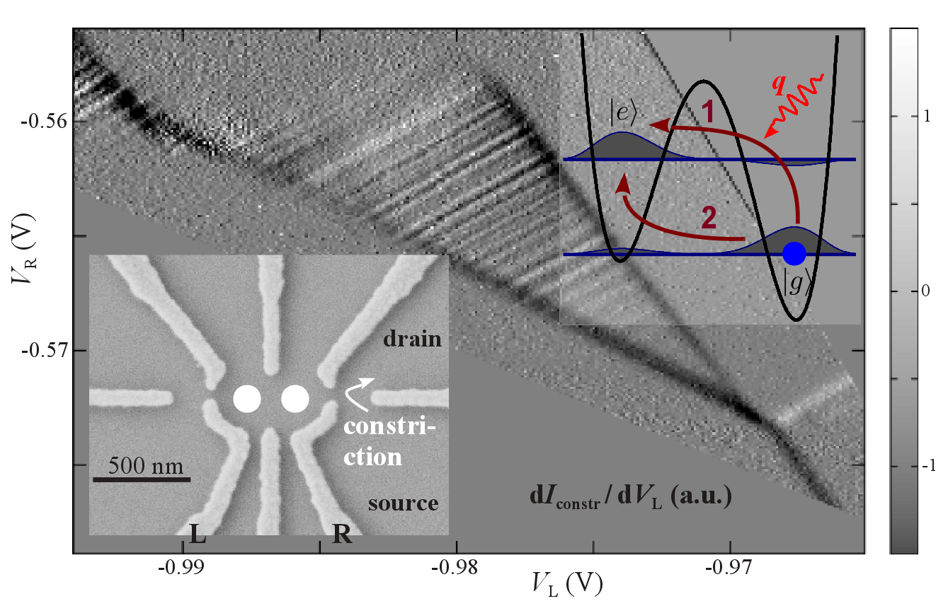
Figure 1. The figure illustrates an example of a single phonon interference effect as observed in the charge stability diagram of a double quantum dot. The lower inset shows a scanning electron microscope image of the AlGaAs/GaAs heterostructure containing a two-dimensional electron system 80 nm beneath the surface. The light gray regions are metal gates used to electrostatically define a double quantum dot (white circles) and two narrow constrictions. For charge sensing we apply a source drain voltage across the right narrow constriction, which is tuned to act as a tunnel barrier, and we detect the linear response of the tunneling current Iconstr (white arrow) while the voltage VL applied to the left plunger gate is slightly modulated. The main figure plots the resulting transconductance dIconstr / dVL as a function of plunger gate voltages VL and VR of the double quantum dot at a temperature of 30 mK. Local extrema (dark and bright lines) indicate changes in the average charge occupation of the double quantum dot (from zero to one electrons). The striped triangle indicates a non-equilibrium configuration. Its origin results from the absorption of single phonons. In our experiment the phonons originate from charge fluctuations in the narrow constriction. The upper inset in the figure sketches the absorption process. In the presence of a finite energy detuning a phonon can be absorbed in either one of the two dots via inelastic tunneling. The resulting two absorption paths indicated by red arrows in the inset acquire a phase-difference which depends on the double quantum dot detuning. In our example the stripe pattern of the non-equilibrium triangle is interpreted as interference fringes caused by the absorption/detection of one phonon at a time.
[1] G. Granger, D. Taubert, C. E. Young, L. Gaudreau, A. Kam, S. A. Studenikin, P. Zawadzki, D. Harbusch, D. Schuh, W. Wegscheider, Z. R. Wasilewski, A. A. Clerk, S. Ludwig, A. S. Sachrajda, Nature Phys. 8, 522 (2012).
Large Nuclear Spin Polarization in Gate-Defined Quantum Dots Incorporating a Single-Domain Nanomagnet
Gunnar Petersen, Eric A. Hoffmann and Stefan Ludwig,
in collaboration with Dieter Schuh (University of Regensburg), Werner Wegscheider (ETH Zürich) and Geza Giedke (MPQ, Garching)
The long-term goal of using laterally defined double quantum dots (QD) in GaAs/AlGaAs heterostructures for quantum information applications has recently been brought closer by many experiments demonstrating the capability of this system. The most advanced experiments used two-electron molecular states as the basis states of a spin qubit and demonstrated initialization, readout and coherent manipulation capabilities. It turns out that, on the one hand, these spin qubit's coherence time is largely limited by the hyperfine interaction of the electrons confined in the dots with many thermally fluctuating host nuclei. On the other hand, the hyperfine interaction also opens up new possible applications, as it provides access to the nuclear spins which have very long coherence times and could e.g. serve as quantum memory.
We investigate the complex electron-nuclear spin dynamics caused by the hyperfine interaction in a system combining a single-domain nanomagnet and a GaAs/AlGaAs double QD defined by electrostatic gates (see fig. 1a). As we find out, the nanomagnet enhances our ability to manipulate the nuclear spin ensemble using the hyperfine interaction. We manipulate the nuclei in a simple transport experiment by driving a current through the double QD. Due to spin conservation triplet states tend to block the current (Pauli-spin blockade) unless they are mixed with singlet states either by a field gradient ∇B introduced by the nanomagnet or by the hyperfine interaction (see fig. 1b). The leakage current component related to the hyperfine interaction involves electron-nuclear spin flip-flop processes and can cause a dynamic polarization of the nuclear spins. The overall dynamics is complex but can be captured in a semi-classical rate equation model. Our model describes two fixed points of constant polarization P, where one of them can be adjusted by an applied external field Bext (see fig. 1c). Therefore, once the system is initialized at this "adjustable" fix point, the polarization can be dragged to higher values by increasing Bext up to a value Pmax indicated by a maximum in leakage current (see fig. 2a). Figure 2c plots the leakage current during the dragging procedure performed at different gate voltage configurations (fig. 2b). The current peaks marked by arrows indicate the maximally reached polarization. By this technique we achieve a maximum polarization of ~50 % (lowest trace in fig 2c) unrivaled in lateral QD systems.
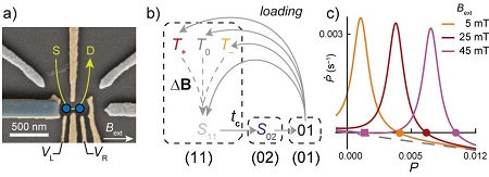
Figure 1. a) Scanning electron micrograph of the sample surface showing the gate layout used to define the double QD by electrostatic gates (light orange) and a single domain nanomagnet on top of the left most gate (light blue). b) Current cycle for electrons passing the double QD, where (mn) indicates the number, m (n), of electrons in the left (right) dot. More in the main text. c) Phenomenological model sketched for three different Bext. Circles indicate the "adjustable" fix point.
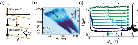
Figure 2. a) Sketch of the dragging procedure used to generate large polarizations. b) Leakage current bias triangle for the Pauli spin blockade regime. The position for dragging measurements in c) are indicated by color coded circles and a triangle. c) Dragging experiment for various positions indicated in b) and offset for clarity. Sharp current peaks (marked by arrows) correspond to the maximum polarization, Pmax in a).
[1] G. Petersen, E. A. Hoffmann, D. Schuh, W. Wegscheider, G. Giedke,and S. Ludwig, arXiv:1212.3140
Few electron double quantum dot in an isotopically purified 28Si quantum well
Stefan Ludwig,
in collaboration with A. Wild, J. Sailer, G. Abstreiter (Technische Universität München), J. Kierig, D. Bougeard (University of Regensburg), J. W. Ager, E. E. Haller (Lawrence Berkeley National Lab and University of California)
Silicon based quantum dot systems are promising hosts for spin-qubits as it is possible to engineer quantum wells virtually free of nuclear spins in this material. They indeed promise much longer coherence times compared to the very common GaAs-based spin qubits, which suffer from decoherence induced by the hyperfine interaction of the qubits electron spin with many thermally fluctuating nuclear spins. This collaboration aims at using lateral quantum dots for spin qubits defined in the high mobility two-dimensional electron system (2DES) of isotopically purified 28Si/SiGe-heterostructures. In 2012 we have demonstrated the feasibility of our goal as we have demonstrated the high quality of our isotopically purified 28Si/SiGe-heterostructures as well as our ability to laterally define a fully tunable few electron double quantum dot in this material system.
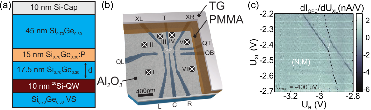
Figure 1. (a) Layer sequence of the 28Si/SiGe-heterostructure. A 28Si-quantum well (which contains the 2DES) is embedded into a natural SiGe host crystal and separated by a spacer of thickness d = 17.5 nm from the SiGe:P doping layer. (b) Layer stack of the device and electron beam defined gate layout. Dark gray areas are metal gates which are negatively charged in order to locally deplete the 2DES beneath and thereby define the fully tunable double quantum dot. In addition a global top gate (TG) covers the entire nanostructure. It is electrically isolated from the other gates by cross-linked PMMA (plexiglass). The approximate position of the two tunnel coupled dots are sketched with white ellipses. Roman numbers denote Ohmic contacts used for transport measurements. (c) Charge stability diagram of the double quantum dot showing the transconductance of a capacitively coupled quantum point contact as charge detector. Dark (bright) lines are the charging (charge reconfiguration) lines of the two dots. Crossing these lines corresponds to changing the charge of one (both) dot(s) by exactly one electron. We have evidence that both dots are uncharged in the area marked by (m,n).
[1] A. Wild, J. Kierig, J. Sailer, J. W. Ager, E. E. Haller, G. Abstreiter, S. Ludwig, and D. Bougeard, Appl. Phys. Lett. 100, 143110 (2012)
Optical and optoelectronical phenomena in nanodevices
Very different nanosystems ranging from electrostatically defined traps to DNA-assembled nanohelices were used to study optical phenomena in nanodevices. Spatially indirect excitons in double quantum wells were trapped and studied in optical experiments at sub-Kelvin temperatures. In this novel experimental regime the thermal de Broglie wavelength of confined excitons becomes comparable to the exciton-exciton separation. On the one hand this is very attractive for studies of correlation effects, and on the other hand it allows the realization of few-exciton traps confining down to a single indirect exciton. Nuclear spin phenomena of single neutral and charged excitons confined in self-assembled dots were another subject of investigation. Resonant laser spectroscopy was used to optically pump nuclear spins with the remarkable finding of nuclear spin induced resonance feedback that leads to dragging. We identified quadrupolar effects in strained self-assembled dots as a crucial ingredient to our quantitative model to describe the dragging phenomena. Our collaborative research project on DNA-origami assembly of photofunctional nanosystems has resulted in the demonstration of strong circular dichroism and optical rotatory dispersion of artificial nanohelices. In our studies of optical properties of individual carbon nanotubes we demonstrated that as-grown suspended nanotubes have superior spectral properties arising from bright, long-lived and coherent localized excitons.
Confinement and interaction of single indirect excitons in a voltage-controlled trap formed in double InGaAs quantum wells
Georg J. Schinner, Jens Repp, Enrico Schubert and Jörg P. Kotthaus
in collaboration with Andreas D. Wieck (Ruhr-Universität Bochum), Alexander O. Govorov (Ohio University) and Alexander W. Holleitner (Technische Universität München)
We perform photoluminescence measurements on electrostatically trapped dipolar excitons in an InGaAs-Double Quantum Well (DQW). In our experimental setup the exciton generation is separated from the trapping area where the photoluminescence spectroscopy measurements are done. With a 3He refrigerator with a base temperature below 240mK it is possible to cool down the exciton gas to a regime where the thermal de Broglie wavelength becomes comparable to the exciton-exciton separation [1].
The diameter of the smallest trapping gates is in the order of some hundred nanometers (See Fig. 1c). In these traps the transition from confined multi excitons down to a single, electrostatically trapped indirect exciton can be studied. In the few exciton regime, we observe discrete emission lines identified as resulting from a single dipolar exciton, a biexciton and a triexciton, respectively (See Fig 2).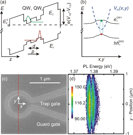
Figure 1. (a) Scheme of the DQW band gap within a field effect device. EC and EV denote the conduction and valence band edge, respectively. The electron and hole wavefunctions of the ground states hhQW21 and eQW11 are indicated. The energetic tilt of the DQW is tuned by the gate voltages VT;G with respect to the flat band voltage VFB ≈ 0.75 V. (b) in-plane variation of the hhQW21 and eQW11 ground state and the resulting confinement potential VIX. (c) displays a scanning electron micrograph of the gate pattern. (d) logarithmically displays the PL intensity vs. energy and position y at x =0 [VG = 0.75 V, VT = 0.25 V, TLattice = 242 mK, PLaser =2.8 nW, ELaser = 1.494 eV].
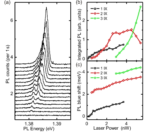
Figure 2. (a) PL spectra for different occupations of the trap nonlinearly changed by laser power between 55pW and 10 nW. In comparison to the emission from individual self-assembled InGaAs quantum dots PL counts in the single exciton limit are typically found to be 1000-fold lower, reflecting the correspondingly increased radiative lifetime of IX. The corresponding integrated PL intensity and PL blue shift is shown in (b) and (c) [VG = 0.65 V, VT = 0.30 V, TLattice = 245 mK, ELaser = 1.494 eV].
[1] G.J. Schinner et al., arXiv: 1111.7175 (2011) and Phys. Rev. B in press.
[2] G.J. Schinner et al., Phys. Rev. Lett. 110, 127403 (2013).
Dynamic nuclear spin polarization in the resonant laser excitation of a quantum dot
Alexander Högele
in collaboration with M. Kroner, C. Latta, M. Claassen, I. Carusotto and A. Imamoglu
Our previous and more recent studies of nuclear spin effects in quantum dots have identified resonant laser spectroscopy as a new regime of dynamic nuclear spin polarization. Resonant optical excitation of lowest-energy excitonic transitions in self-assembled quantum dots leads to nuclear spin polarization that is qualitatively different from the well known optical orientation phenomena. By carrying out a comprehensive set of experiments, we demonstrate that nuclear spin polarization manifests itself in quantum dots subjected to finite external magnetic field as locking of the higher energy Zeeman transition to the driving laser field, as well as the avoidance of the resonance condition for the lower energy Zeeman branch. We interpret our findings on the basis of dynamic nuclear spin polarization originating from non-collinear hyperfine interaction and find excellent agreement between experiment and theory. Our results provide evidence for the significance of non-collinear hyperfine processes not only for nuclear spin diffusion and decay but also for buildup dynamics of nuclear spin polarization in a coupled electron-nuclear spin system.
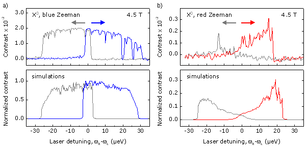
Figure 1. Signatures of dynamic nuclear spin polarization in resonant laser spectroscopy of a neutral exciton in a single quantum dot at 4.2 K in a finite magnetic field of 4.5 T. (a) and (b) show differential transmission spectra (upper panel) and results of the simulations (lower panel) for the blue and red branches of the Zeeman-split X0 transition. The blue Zeeman branch is actively locked on-resonance with the laser (laser scan directions indicated by arrows) by the Overhauser shift arising from dynamic nuclear spin polarization. The resulting lineshape exhibits a flat-top form, an effect referred to as dragging. On the contrary, the red Zeeman branch avoids the resonance by nuclear spin polarization feedback as evidenced by the triangular lineshape of anti-dragging.
[1] C. Latta et al., Nature Physics 5, 758 (2009).
[2] A. Högele et al., Phys. Rev. Lett. 108, 197403 (2012).
DNA-based self-assembly of chiral plasmonic nanostructures with tailored optical response
Alexander Högele
in collaboration with A. Kuzyk, R. Schreiber, Z. Fan, G. Pardatscher, E.M. Roller, F.C. Simmel, A.O. Govorov and Tim Liedl
Matter structured on a length scale comparable to or smaller than the wavelength of light can exhibit unusual optical properties. Particularly promising components for such materials are metal nanostructures, where structural alterations provide a straightforward means of tailoring their surface plasmon resonances and hence their interaction with light. However, top-down fabrication of plasmonic materials with controlled optical responses in the visible spectral range remains challenging, because lithographic methods are limited in resolution and in their ability to generate genuinely three-dimensional architectures. Molecular self-assembly provides an alternative bottom-up fabrication route not restricted by these limitations. We show that DNA origami enables the high-yield production of plasmonic structures that contain nanoparticles arranged in nanometre-scale helices [1]. We find, in agreement with theoretical predictions, that the structures in solution exhibit defined circular dichroism and optical rotatory dispersion effects at visible wavelengths that originate from the collective plasmon-plasmon interactions of the nanoparticles positioned with an accuracy better than two nanometres. In accord with theory, the optical response of our nanoparticle assemblies is rationally designed and tunable in handedness, colour and intensity.
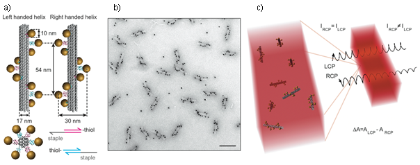
Figure 1. (a) Left- and right-handed nanohelices are formed by nine gold nanoparticles that are attached to the surface of DNA origami 24-helix bundles. (b) TEM image of assembled left-handed gold nanohelices (scale bar, 100 nm). (c) Nanohelices exhibit giant circular dichroism that is measured as the difference in absorbance of left-hand-circularly polarized (LCP) and right-hand-circularly polarized (RCP).
[1] A. Kuzyk et al., Nature 483, 311-314, 758 (2009).
Optical signatures of quantum dot excitons in carbon nanotubes
Matthias S. Hofmann, Jan T. Glückert and Alexander Högele
We report on optical studies of quantum dot excitons in individual suspended carbon nanotubes at cryogenic temperatures [1]. Narrow optical linewidths, strongly suppressed spectral wandering, and photoluminescence lifetimes in the range of nanoseconds emerge as key signatures of exciton localization. Moreover, localization inhibits exciton diffusion and protects the exciton from dephasing by structural or environmental inhomogeneities as well as from exploring nonradiative quenching sites. In consequence, quantum dot excitons in carbon nanotubes are long-lived, bright and coherent.
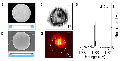
Figure 1. (a) Transmission and (b) scanning electron micrographs with cross-section schematics of sample regions with carbon nanotubes suspended over a hole and a silicon oxide crater of 200 nm depth, respectively. False-color maps recorded in reflection (c) and photoluminescence (d) for a single carbon nanotube with a sharp emission spectrum (e). The linewidth at 4.2 K is limited to 40 µeV by the resolution of our spectrometer. Dashed white circles in (c) and (d) indicate the perimeter of the circular crater. Scale bars in (a) - (d) are 500 nm.
[1] M. S. Hofmann, J. T. Glückert, and A. Högele, arXiv:1209.3429 (2012).
Nanomechanical systems
In the year 2012, we have continued our research on nanomechanical systems, freely suspended nanostructures with nanoscale cross-sections and lengths of up to several 10 microns. In particular, significant progress has been achieved in controlling and detecting the mechanical modes of such nanoscale resonators. This represents a major breakthrough, as it is an important prerequisite for applications of nanomechanical resonators in fundamental experiments or sensing devices.
As in previous years, we have employed doubly clamped string resonators fabricated from high stress silicon nitride as high Q nanomechanical systems and obtained room temperature quality factors exceeding 300,000. The well-established chip layout incorporating electrodes for dielectric coupling to the resonator has been refined, and now allows combining dielectric actuation, manipulation and detection, enabling full dielectric transduction. Several electrode geometries have been investigated, allowing detailed insights into the tuning behavior of the two orthogonal flexural modes of the strings. A geometry could be identified which allows bringing both modes into resonance where strong coupling of the two modes mediated by the dielectric gradient field is observed. This discovery marked the starting point of a new research effort, focussing on non-adiabatic dynamics of strongly coupled nanomechanical resonator modes. After incorporating pulsed measurement schemes to analyze the time-dependend evolution of nanomechanical modes, Landau-Zener transitions as well as coherent control of a nanomechanical system have been investigated.
In an attempt to scale down the size of the nanomechanical resonators under investigation, freely suspended carbon nanotubes haven been fabricated. To directly probe their vibrations, a high finesse optical microcavity has been employed. Large optomechanical coupling is observed after inserting the nanotube into the cavity mode. This allows to directly probe the Brownian motion of the nanotube in the optical frequency noise spectrum.
Frequency and Q factor control of nanomechanical resonators
Johannes Rieger, Thomas Faust, Maximilian J. Seitner, Jörg P. Kotthaus and Eva M. Weig
We present an integrated scheme for dielectric drive and read-out of high-Q nanomechanical silicon nitride string resonators which enables tuning of both the resonance frequency and the quality factor with an applied dc voltage [1]. Comparing the two sample geometries schematically depicted in Fig. 1 reveals that the electrode design crucially affects the tuning behavior: Whereas the vertical electrode offset determines the direction of frequency tuning for the flexural out-of-plane mode of a string resonator (see "lowered" and "elevated" electrode layout, Fig. 1), the in-plane-mode is not susceptible to such a change in geometry.
Furthermore we show that the damping constant is also altered by the applied dc voltage, such that the mechanical quality factor can be voltage reduced more than fivefold. This effect can be explained by dielectric damping in the resonator material. A simple model incorporating the resonator’s complex electric polarizability and position in an inhomogeneous electric field is derived, which agrees very well with experimental results (Fig. 2). The demonstrated findings open up the possibility to exert Q factor control via an applied dc voltage, without the need of any active electronics such as a phase-locked loop. This technology could significantly increase the bandwidth of NEMS sensors, leading to much more adaptable devices.
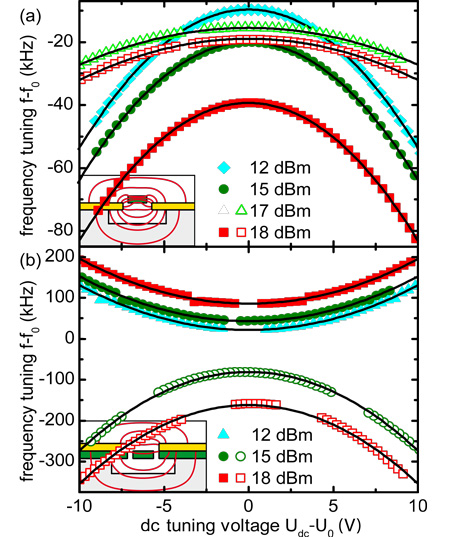
Figure 1. Quadratic tuning of the mechanical resonance frequency with dc voltage and fitted model. In-plane-mode data are depicted as open, out-of-plane data as filled symbols. a) Both modes tune in the same direction for the "lowered electrode" sample geometry depicted in the inset. b) The modes tune in opposite direction for the "elevated electrode" geometry.
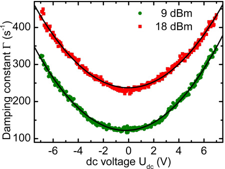
Figure 2. Damping constant versus dc voltage for two different microwave powers, exhibiting a quadratic behavior. The solid lines are a fit of our model.
[1] J. Rieger, T. Faust, M. J. Seitner, J. P. Kotthaus, and E. M. Weig, Appl. Phys. Lett. 101 103110 (2012)
Nonadiabatic dynamics of two strongly coupled nanomechanical resonator modes
Thomas Faust, Johannes Rieger, Maximilian J. Seitner, Peter Krenn, Jörg P. Kotthaus and Eva M. Weig
The Landau-Zener transition [1,2] is a fundamental concept for dynamical quantum systems and has been studied in numerous fields of physics. Here we present a classical nanomechanical model system exhibiting analogous behaviour [3].
A system with two tunable energy levels is realized using the two orthogonal flexural modes of a doubly clamped high stress silicon nitride string depicted in Fig. 1(a). Dielectric coupling to a microwave readout cavity provides a sensitive detection scheme [4]. In addition, the same electrodes are employed to actuate and tune the resonances via electric gradient fields. For the chosen device layout, this allows to bring the two modes into resonance and observe an avoided crossing (Fig. 1(b)). The extracted coupling strength is much larger than the linewidth of the mechanical resonances, thus the system is clearly in the strong-coupling regime.
A pulsed measurement scheme is used to analyze the time-dependent evolution of a previously initialized mode as it is swept across the coupling region. At lower sweep rates, the system adiabatically follows the energy eigenstates, whereas the energy is transferred from one branch to the other during very fast sweeps. The measured transition probabilities show an excellent quantitative agreement with the Landau-Zener theory (Fig. 2). In addition, coherent control of the nanomechanical system is demonstrated, as the energy relaxation time of our system exceeds the length of the manipulation pulses.
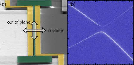
Figure 1. Panel (a) shows a SEM micrograph of the silicon nitride beam and the adjacent electrodes, the arrows denote the two flexural modes. The avoided crossing between the modes is shown in (b).
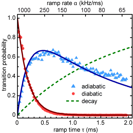
Figure 2. Measured adiabatic and diabatic transition probabilities are plotted along with the theoretical predictions (solid lines). The dashed green line is the decay probability, ensuring that the sum of all three lines is constant.
[1] L. D. Landau, Phys. Z. Sowjetunion 2, 46 (1932).
[2] C. Zener, Proc. R. Soc. London, Ser. A 137, 696 (1932).
[3] T. Faust, J. Rieger, M.J. Seitner, P. Krenn, J.P. Kotthaus and E.M. Weig, Phys. Rev. Lett. 109, 037205 (2012).
[4] T. Faust, P. Krenn, S. Manus, J.P. Kotthaus, and E.M. Weig, Nat. Commun. 3, 728 (2012).
Cavity-enhanced optical detection of carbon nanotube Brownian motion
Sebastian Stapfner, Lukas Ost and Eva M. Weig
in collaboration with David Hunger (LMU München), Jakob Reichel (ENS Paris), Ivan Favero (MPQ Paris Diderot 7)
Directly probing the mechanical motion of nanoscale objects is a challenging task because of their small dimensions. One example for such molecular scale mechanical resonators are freely suspended, doubly clamped carbon nanotubes (CNTs) with resonance frequencies in the hundred kilohertz range. To detect the vibration of such a CNT a fiber-based optical micro cavity is employed, as small mode volume optical cavities of high finesse are precise instruments to read out the mechanical motion of objects much smaller than the optical wavelength.
Measurements are carried out in vacuum 10-5 mbar and at room temperature (300 K). Deflections of the CNT down to 50 pm/Hz1/2 ± 50 % are optically resolved by probing the cavity reflexion. This sensitivity is sufficient to observe the Brownian motion [1] of a pronounced CNT resonance at 0.51 MHz (Fig. 1(a), red trace). In addition, a piezo-driven vibrational spectrum of the CNT is recorded in the cavity (Fig. 1(a), gray trace). The same piezo-driven device is monitored in the scanning electron microscope (SEM), independently confirming the most pronounced spectral features (Fig. 1(a), black arrows) as mechanical resonances (Fig. 1(b) and (c)).
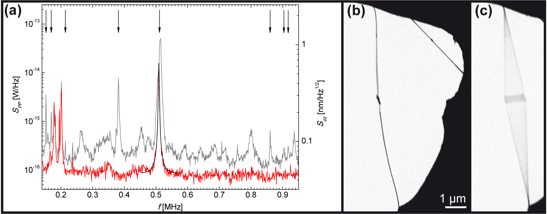
Figure 1. (a) Vibrational spectra of the CNT in the cavity with and without actuation through an external piezo (gray and red trace, respectively). The Lorentzian fit (black) refers to the resonance at 0.51 MHz in the undriven spectrum (red) and yields a quality factor of 300. The calibration of the deflection is deduced from the thermal noise spectrum (red) via the equipartition theorem within a 50 % error margin. The black arrows highlighting additional resonances in the driven spectrum (gray) indicate mechanical modes that were independently recovered in complementary SEM measurements. Processed SEM images of (b) the undriven CNT and of (c) the vibrating CNT driven at 518 kHz.
[1] S. Stapfner, L. Ost, D. Hunger, J. Reichel, I. Favero, and E. M. Weig, Appl. Phys. Lett. 102 151910 (2103).
Bachelor theses completed in 2012
- Jan David Beitner
“Absorption in High-Q Silica Microcavities” - Dominic Berchtold
“Tieftemperaturspektroskopie einzelner CdTe/CdSe Quantenpunkte in einer Polymer-Matrix” - Christoph Berger
“Seebeck and Peltier effects: experimental setup and results” - Maximilian Gerer
“Current through a double quantum dot in the spin-blockade regime: Theoretical models and simulations” - Todor Krastev
“Entwicklung und Optimierung von Mikrowellenresonatoren zur dielektrischen Detektion von schwingenden SiN-Nanobalken” - Sophie Ratcliffe
“Developing a resonant waveguide cavity as a notch filter”
Master theses completed in 2012
- Benjamin Gmeiner
“Nanomechanical resonators in the strong coupling regime” - Patrick Loch
“Beugungsdetektion zweidimensionaler GaAs-Säulengitter in verschiedenen Umgebungsmedien” - Tobias Mittereder
“Diffraction measurements on a lattice of actuated nanomechanical GaAs pillars” - Maximilian Seitner
“Mechanische und dielektrische Manipulation nanomechanischer Resonatoren”
Diploma theses completed in 2012
- Anna Eder
“Tieftemperaturexperimente an mesoskopischen Systemen im Nichtgleichgewicht” - Johannes Schmelzl
“Optomechanik nanostrukturierter SiN-Membranen in einer faserbasierten Fabry-Pérot Kavität”
PhD theses completed in 2012
- Georg Schinner
“Correlated behavior of electrostatically trapped dipolar excitons at low temperatures” - Daniela Taubert
“Electronic transport experiments on low-dimensional nanostructures at non-equilibrium conditions”
Guest scientists in 2012
- Prof. Alexander V. Chaplik
Institute of Semiconductor Physics, Novosibirsk, Russland, Alexander von Humboldt Stiftung - Ivan Favero
Université Paris Diderot, France. - Prof. Alexander O. Govorov
Ohio University, Athens, OH, USA, SFB 631 - Prof. Alexander Holleitner
Technische Universität München, Walter Schottky Institut - Prof. Andreas Isacsson
Chalmers University of Technology - Prof. Khaled Karraï
Technische Universität München and attocube Systems AG, München - Prof. Efrat Lifshitz
Technion-Israel Institute of Technology, Haifa, Israel - Prof. Dr. Mansour Shayegan
Princeton University, USA, Alexander von Humboldt Stiftung - Dr. Eric Hoffmann
Physics Department & Material Science Institute, University of Oregon, USA, Alexander von Humboldt Stiftung - Dr. Tomohiro Yamaguchi
Advanced Device Laboratory, RIKEN Institute of Technology, Tokyo, Japan - Johannes Kierig
Institut für Experimentelle und Angewandte Physik, Universität Regensburg - Andreas Wild
Technische Universität München, Walter Schottky Institut
Group members in 2012
Senior scientists
- Prof. Jörg P. Kotthaus
- Prof. Alexander Högele
- Dr. Heribert Lorenz
- Dr. Stefan Ludwig
- Dr. Eva-Maria Weig
- Dr. Onur Basarir
- Dr. Katarzyna Kowalik-Seidl
- Dr. Darren Southworth
- Dr. Philipp Paulitschke
Secretary
- Martina Jüttner
Technical staff
- Philipp Altpeter
- Anton Heindl
- Stephan Manus
- Reinhold Rath
Ph.D. students
- Thomas Faust
- Florian Forster
- Jan Tibor Glückert
- Matthias Hauck
- Matthias Hofmann
- André Neumann
- Gunnar Petersen
- Platonov Sergey
- Jens Repp
- Johannes Rieger
- Georg Schinner
- Enrico Schubert
- Florian Seilmeier
- Sebastian Stapfner
- Daniela Taubert
- Nooshin Yavarina
Diploma and Master students
- Anna Eder
- Benjamin Gmeiner
- Max Falkowski
- Patrick Loch
- Simon Mates
- Sybille Meyer
- Tobias Mittereder
- Johannes Schmelzl
- Maximilian Seitner
Bachelor students
- Jan David Beitner
- Dominic Berchtold
- Christoph Berger
- Maximilian Berger
- Todor Kastev
- Sophie Ratcliffe
Publications in 2012
- K. Kowalik-Seidl, X. P. Vögele, B. N. Rimpfl, G. J. Schinner, D. Schuh, W. Wegscheider, A. W. Holleitner, and J. P. Kotthaus
“Tunable Photoemission from an Excitonic Antitrap”
Nano Lett. 12, 326 (2012). - T. Faust, P. Krenn, S. Manus, J.P. Kotthaus, and E.M. Weig
“Microwave cavity-enhanced transduction for plug and play nanomechanics at room temperature”
Nat. Commun. 3, 728 (2012) - A. Högele, M. Kroner, C. Latta, M. Claassen, I. Carusotto, C. Bulutay, and A. Imamoglu
“Dynamic nuclear spin polarization in the resonant laser excitation of an InGaAs quantum dot”
Phys. Rev. Lett. 108, 197403 (2012) - T. Faust, J. Rieger, M. J. Seitner, P. Krenn, J. P. Kotthaus, and E. M. Weig
“Nonadiabatic Dynamics of Two Strongly Coupled Nanomechanical Resonator Modes”
Phys. Rev. Lett. 109, 037205 (2012) - G. Granger, D. Taubert, C. E. Young, L. Gaudreau, A. Kam, S.A. Studenikin, P. Zawadzki, D. Harbusch, D. Schuh, W. Wegscheider, Z. R. Wasilewski, A. A. Clerk, S. Ludwig, and A. S. Sachrajda
“Quantum interference and phonon-mediated back-action in lateral quantum-dot circuits”
Nature Phys. 8 522 (2012) - M. Yu. Melnikov, J. P. Kotthaus, V. Pellegrini, L. Sorba, G. Biasiol, and V. S. Khrapai
“Influence of e-e scattering on the temperature dependence of the resistance of a classical ballistic point contact in a two-dimensional electron system”
Phys. Rev. B 83 075425 (2012) - J. Rieger, T. Faust, M. J. Seitner, J. P. Kotthaus, and E. M. Weig
“Frequency and Q factor control of nanomechanical resonators”
Appl. Phys. Lett. 101 103110 (2012) - D. R. Koenig, and E. M. Weig
“Voltage-sustained self-oscillation of a nano-mechanical electron shuttle”
Appl. Phys. Lett. 101 213111 (2012) - C. Baker, S. Stapfner, D. Parrain, S. Ducci, G. Leo, E. M. Weig, and I. Favero
“Optical instability and self-pulsing in silicon nitride whispering gallery resonators”
Opt.Express 20 29076 (2012) - M. Stallhofer, C. Kastl, M. Brändlein, D. Schuh, W. Wegscheider, J. P. Kotthaus, G. Abstreiter, and A. W. Holleitner
“Enlarged magnetic focusing radius of photoinduced currents in mesoscopic circuits”
Phys. Rev. B 86 115315 (2012) - A. Wild, J. Kierig, J. Sailer, J. W. Ager, E. E. Haller, G. Abstreiter, S. Ludwig, and D. Bougeard
“Few electron double quantum dot in an isotopically purified 28Si quantum well”
Appl. Phys. Lett. 100, 143110 (2012) - A. Kuzyk, R. Schreiber, Z. Fan, G. Pardatscher, E.-M. Roller, A . Högele, F.C. Simmel, A.O. Govorov, T. Liedl
“DNA-based self-assembly of chiral plasmonic nanostructures with tailored optical response”
Nature 483 311-314 (2012) - M. Handloser, R.B. Dunbar, A. Wisnet, P. Altpeter, C. Scheu, L. Schmidt-Mende, and A. Hartschuh
“Influence of metallic and dielectric nanowire arrays on the photoluminescence properties of P3HT thin films”
Nanotechnology 23 305402 (2012)
Awards in 2012
- Stefan Ludwig
CeNS Publikationspreis 2012. - Alexander Högele
CeNS Publikationspreis 2012. - Thomas Faust, Jörg Kotthaus , Eva Weig
CeNS Publikationspreis 2012.
Invited talks in 2012
Jörg P. Kotthaus
- “Spectroscopy of electrostatically trapped dipolar excitons: From correlated ensembles to individual excitons”
17th Int. Winterschool “New Developments in Solid State Physics”
Mauterndorf, Austria
February 2012
- “Nanomechanical resonantors - improving coherence and transduction”
Humboldt Kolleg NS&T'12: Nanoscale Science and Technology
Hammamet, Tunisia
March 2012
- “Nanomechanical resonators - coherent control of nanomechanical motion”
Yearly Meeting Swiss Physical Society
Zurich, Switzerland
June 2012
- “Single exciton manipulation in gate-defined quantum traps”
European Workshop on Indirect Excitons
Barcelona, Spain
December 2012
Stefan Ludwig
- “Manipulation of Nuclear Spins in Quantum Dots using a Single Domain Nanomagnet”
Physikalisches Kolloquium der Universität Regensburg
Regensburg, Germany
January 2012
- “Nuclear Spin Manipulation in GaAs Based Quantum Dots using a Single Domain Nanomagnet”
SPP1285 International Workshop on “Spin and Quantum Transport”
Berlin, Germany
March 2012
- “Manipulation of Nuclear Spins in Quantum Dots Using a Single Domain Nanomagnet”
2012 EMN (Energy Materials Nanotechnology) Meeting
Orlando, USA
April 2012
- “Quantum Interference and Phonon-Mediated Back-Action in Nanoscale Devices”
QC2/QSIT Seminar (Nano and Quantum Physics)
Basel, Switzerland
May 2012
- “Microscopic Origin of the 0.7 Anomaly in Quantum Point Contacts”
APCTP-ICTP Joint Conference (SM-12/68) on Quantum Transport through Nanostructures
Pohang, Korea
August 2012
- “Coherent Phenomena in Mesoscopic Structures”
2012 Cambridge–ITAP School and Workshop on Coherence and Condensation in Low Dimensional Systems
Turunc (Marmaris), Turkey
September 2012
- “Quantum Interference and Phonon-Mediated Back-Action in Nanoscale Devices”
Colloquium Division 2, Physikalisch Technische Bundesanstalt (PTB)
Braunschweig, Germany
October 2012
Alexander Högele
- “Quantum optics in single carbon nanotubes”
Focus Workshop “THz dynamics in carbon based nanostructures”, Helmholtz-Zentrum
Dresden, Germany
March 2012
- “Long-lived Excitons in Pristine Carbon Nanotubes”
Fakultät für Physik, LMU München, LS Hänsch, Laser Spectroscopy & Quantum Physics Group
Munich, Germany
April 2012
- “Optical properties of freely suspended carbon nanotubes at cryogenic temperatures ”
221st ECS Meeting
Seattle, WA, USA
May 2012
- “Cryogenic spectroscopy of suspended carbon nanotubes”
Kavli Nanoscience Seminar, Kavli Institute of Nanoscience at TU Delft
Delft, Netherlands
June 2012
- “Quantum dot excitons in carbon nanotubes”
International CeNS Workshop 2012, Venice International University
Venice, Italy
September 2012
- “Quantum dots in carbon nanotubes: a new model system for solid-state quantum optics”
Fakultät für Physik, LMU München, LS Bloch, Quantum Optics Group
Munich, Germany
October 2012
Eva M. Weig
- “Self-sustained oscillation of nanomechanical resonators”
Microkelvin Workshop
Smolenice, Slovakia
March 2012
- “Integrated transduction and coherent control of high Q nanomechanical systems using dielectric gradient forces”
DPG Frühjahrstagung, Symposium SYNM 1: Frontiers of Nanomechanics
Berlin, Germany
March 2012
- “Coherent control of strongly coupled nanomechanical systems”
APCTP Workshop on Electrons, Photons and Mechanics on Mesoscopic Scales
Pohang, Korea
August 2012
- “Opto-mechanical resonators”
Son et Lumière: from microphotonics to nanophononics
Les Houches, France
September 2012
Senior scientists of cooperating groups
- Gerhard Abstreiter+, Max Bichler
Walter Schottky Institut, TU München, Garching, Germany. - J.W. Ager, E.E. Haller
Lawrence Berkeley National Laboratory, CA, USA. - Dominique Bougeard
Institut für Experimentelle und Angewandte Physik, University of Regensburg, Germany. - Andrew Cleland
University of California Santa Barbara, CA, USA. - Aashish Clerk
Mc Gill University, Montreal, Canada. - Alik Chaplik
Institute of Semiconductor Physics, Novosibirsk, Russia. - Jan von Delft∗+
Institute for Theoretical Solid State Physics, LMU München, Germany. - Valeri Dolgopolov, Vadim Khrapay
Russian Academy of Sciences, Chernogolovka, Russia. - Ivan Favero
Université Paris Diderot, France. - Niels Fertig∗
Nanion GmbH, München, Germany. - Jonathan J. Finley, Martin S. Brandt, Peter Vogl, Gregor Koblmüller
Walter Schottky Institut, TU München, Garching, Germany. - Hermann Gaub∗+
LMU München, Germany. - Geza Giedke
Max-Planck Institute for Quantum Optics, Garching, Germany. - Alexander O. Govorov
Ohio University, Athens, OH, USA. - Rudolf Groß+, Hans Hübl
Walter Meißner Institut, TU München, Garching, Germany. - Peter Hänggi∗+
Institut für Physik, Universität Augsburg, Germany. - Theodor W. Hänsch+, David Hunger
LMU München, Germany and Max-Planck Institute for Quantum Optics, Garching, Germany. - Achim Hartschuh∗+
LMU München, Germany. - Wolfgang Heckl∗+
Deutsches Museum, München, Germany. - Moty Heiblum, Vladimir Umansky
Weizmann Institute of Science, Rehovot, Israel. - Alexander Holleitner∗+
Walter Schottky Institut, TU München, Garching, Germany. - Peter Hommelhoff
Max-Planck Institute for Quantum Optics, Garching, Germany. - Atac Imamoglu
Department of Physics, ETH Swiss Federal Institute of Technology, Zürich, Switzerland. - Bernd Irmer∗
Nanotools, Germany. - Andreas Isacsson
Chalmers University of Technology, Sweden. - Koji Ishibashi+
Advanced Device Laboratory, RIKEN Institute of Technology, Tokyo, Japan. - Khaled Karraï∗
attocube Systems and LMU München, Germany. - Tobias Kippenberg+
Max-Planck Institute for Quantum Optics, Garching, Germany and École Polytechnique Fédérale de Lausanne, Switzerland. - Tim Liedl∗+
LMU München, Germany. - Efrat Lifschitz
Technion, Haifa, Israel. - Joachim Rädler∗+, Doris Heinrich+, Bert Nickel∗+
LMU München, Germany. - Jakob Reichel
École normale supérieure, Paris, France. - Andrew Sachrajda
Institute for Microstructural Sciences, National Research Council, Ottawa, Canada. - Dieter Schuh
Institut für Angewandte und Experimentelle Physik, Universität Regensburg, Germany. - Mansour Shayegan
Princeton University, USA. - Afif Siddiki
Istanbul University, Science Faculty, Physics Department, Turkey. - Friedrich Simmel∗+
TU München, Garching, Germany. - Philip Tinnefeld
TU Braunschweig, Germany. - Werner Wegscheider
Solid State Physics Laboratory, ETH Swiss Federal Institute of Technology, Zürich, Switzerland. - Andreas Wieck, Dirk Reuter
Lehrstuhl für Angewandte Festkörperphysik, Ruhr-Universität Bochum, Germany. - Wilhelm Zwerger+, Michael Hartmann, Ignacio Wilson-Rae
TU München, Garching, Germany. - Val Zwiller
TU Delft, Delft, Netherlands.
∗ Member of the Center for NanoScience (CeNS), LMU München
+ Member of the Nanosystems Initiative Munich (NIM)
Financial support in 2012
Funding of this work via the following agencies is gratefully acknowledged: