Research report 2003
- Introduction
- Electronic properties
- Towards coupling of single electron states
- Electron-phonon interaction in freely suspended quantum dots
- Primary thermometer formed by Coulomb islands in a suspended silicon nanowire
- Quantum interference in a one-dimensional silicon nanowire
- SAM-assisted assembly of carbon nanotubes on gold electrodes
- Nanostructures for testing molecular wires
- Low-temperature, in situ tunable, uniaxial stress measurements in Semiconductors using a piezoelectric actuator
- Optics with nanostructures
- NEMS
- Nanodevices and bio-templated nanostructures
- Diploma theses in 2003
- PhD theses in 2003
- Guest scientists in 2003
- Group members in 2003
- Publications in 2003
- Invited talks in 2003
- Senior scientists of cooperating groups
- Financial support in 2003
Introduction
Physical properties of nanoscale devices and systems are the major theme of our research. In our work we combine the realization and study of top-down fabricated devices employing techniques derived from semiconductor processing with the exploration of bottom-up assembled systems made via chemical and biochemical routes. Our goals range from a deeper fundamental understanding of physical behavior in the nanometer regime to the realization of novel devices and functions developing and employing various nanotechnologies.
The study of electronic properties of nanoscale systems is motivated by the increasing importance of quantum effects as electronic devices decrease in size and the limitations of scaling of traditional electronic devices such as the Metal-Oxide-Semiconductor Field-Effect-Transistor (MOSFET). Our studies of quantum phenomena aim at finding new ways of information processing. One current major research theme are ways to implement and control quantum bits on the basis of solid state electronic and optical devices and thus lay the ground work for a future quantum information technology. In part this research is embedded in the SFB 631 — a long term research platform on “Solid-State Based Quantum Information Processing”, funded by the German Science Foundation (DFG) since July 2003.
Though MOSFET-based Silicon technology will continue to dominate electronics for at least another decade the search for alternative approaches to electronic functions employing molecular scale units and mechanisms of self-assembly is our motivation for new research projects studying molecular electronics with carbon nanotubes and self-assembled monolayers as well artificial molecular networks and machines based on DNA-directed self-assembly. A major portion of this research is part of a DFG-funded Emmy-Noether junior group headed by Friedrich Simmel.
In the nanometer regime electronic, mechanical and optical properties become often inseparably connected. Therefore we have in recent years increased our activities on studying Nano-Electro-Mechanical Systems, in short NEMS, ranging from fundamental studies of the resonant behavior of nanoscale bridges fabricated out of semiconductors to their development as sensing and actuating devices. Ways to efficiently drive such nanoscale resonators by electric, magnetic, mechanic as well as optically induced forces are one current research aspect. Sensing the mechanical motion with nanometer resolution via capacitance, current or optical reflection is another basic theme of ongoing research.
The particular optical properties of nanoscale systems are most dramatically reflected in the discrete optical emission and absorption spectra of quantum dots. There our research is focused on studying individual quantum dots grown by a self-assembling molecular beam epitaxy process in the group of Pierre Petroff, our long-term collaborator and Humboldt award recipient at UC Santa Barbara. In these studies we employ successfully the possibility of changing the occupation of such self-assembled quantum dots with individual electrons by a gate voltage, a technique developed ten years ago in this collaboration. This is combined with high resolution optical techniques to enable the detailed study of the optical absorption and emission of individual quantum dots as a function of charge, magnetic field and temperature. The fundamental aspect of this research carried out jointly with the group of former CeNS member Richard Warburton at Heriot-Watt University in Edinburgh aims at understanding many body interactions in quantum dots. A more application-oriented goal is the realization of single photon emitters that can generate individual photons on demand and are needed for quantum information processing.
The year 2003 has again seen quite a few changes in our group. Five doctoral and one diploma students have successfully completed their degree and left for attractive industrial positions whereas three graduate students, who have finished their diploma have decided to continue as doctoral students in our group. Robert Blick has left for the attractive position of an Associate Professor at the University of Wisconsin and Stefan Ludwig has joined us after a two year postdoctoral period at Stanford, attracted by the possibility of shifting his major research interests from the low-temperature physics of glasses to quantum phenomena in nanoscale electronic and electromechanical systems. Our long-term technical support team Armin Kriele and Klaus Wehrhahn have moved to Nanotools, one of our four successful start-up companies, while Stefan Schöffberger and Alexander Paul have joined us, attracted more by the training possibilities with our clean room tools than by public service salaries. Quite a few members of our group were invited to present 15 talks at international conferences and workshops and we have successfully published 19 papers in internationally acknowledged journals, a number which by chance is well below our long-term yearly average. We are also happy to report that the four start-up companies Advalytix AG, Attocube Systems, Nanion Technologies GmbH and Nanotools GmbH that were formed in recent years by members of our group increase their business success in a highly competitive world and continue to hire graduates from our group.
Finally, after completing a quarter of a century as the “Semiconductor Group”, originally formed at the University of Hamburg in December 1978 we have decided to start the 26th year 2004 with renaming us to “nanophysics group”, adjusting for the continuous change of focus from semiconductor physics to the more general direction of developing systems and studying condensed matter physics in the nanometer regime. We hope that this report finds many interested readers and enjoy to use this opportunity to thank our many cooperating partners worldwide as well as the generous funding bodies that make our effort in research and education possible. Any feedback our readers may have is welcome.
Munich, May 20th, 2004
Jörg P. Kotthaus
Electronic properties
Quantum dots defined electrostatically via surface gates in a GaAs-AlGaAs heterostructure are considered promising candidates for the implementation of quantum information registers, so-called qubits, in solids. Our low temperature studies of single electron transport through quantum dots aim at realizing well-defined charge and spin states in which the coupling between adjacent quantum dots as well as coupling to the environment can be manipulated in a controlled fashion. One aspect concerns creating and coupling quantum dots with low electron numbers. A second aspect aims at controlling the coupling of spin and charge states via pulsed high frequency radiation fields. Coupling of the quantum dots to the environment via phonons is studied in suspended devices acting as phonon cavities. There we observe phonon blockade of single electron transport, a new type of current suppression mediated by discrete cavity phonons In suspended Si nanowires we studied the temperature dependence of Coulomb-blockade-induced conductance minima for their possible utilization as a primary electron thermometer. The wave nature of electron transport is reflected in characteristic conductance oscillations studied in very narrow Silicon field-effect controlled Si nanowires resulting from electron interference. Non-linear multi-mode ballistic electron transport through lateral nanowires we now have demonstrated to be responsible for the ballistic rectification observed in asymmetric mesoscopic four-terminal junctions on GaAs-AlGaAs heterostructures. Alternatively to top-down fabricated semiconductor nanostructures there exist many efforts to use bottom-up assembled molecular structures for the study and possible utilization of electron transport in nanoscale systems. We presently explore routes to combine top-down fabrication with self-assembly techniques aiming to create and investigate electronic devices out of individual carbon nanotubes as well as mesoscopic ensembles of self-assembled molecules. Additional insight into mesoscopic transport phenomena is gained by the study of its dependence on in-situ tunable strain.
Towards coupling of single electron states
Andreas K. Hüttel, Clemens Rössler, Stefan Ludwig, Robert H. Blick, and J. P. Kotthaus, in cooperation with Dieter Schuh and Werner Wegscheider.
One of the most important prerequisites for quantum-dot based quantum computing schemes is the accessibility of single electron states. We have developed and prepared gate geometries designed to reach the limit of one electron per quantum dot or double quantum dot, targeting both charge [1] and spin qubits [2].
Fig. 1 shows a gate electrode geometry defined by electron beam lithography. Two double quantum dots can be defined in separate circuits. Each dot is optimised for minimal electron number. In addition, a quantum point contact as charge detector has been integrated in a third circuit. This is intended to provide a geometry for versatile charge qubit devices.
As a complementing ansatz, we have developed a combined gate – antenna geometry for probing the effect of magnetic RF signals on quantum dots. In Fig. 2, the strip line loop antenna can be seen above the much smaller quantum dot circuit; it is separated from the underlying gate electrodes by an insulating layer.
Figure 1. Gate geometry designed to define two low electron number quantum double dots
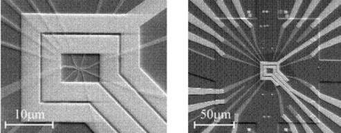
Figure 2. Loop antenna for coupling magnetic RF signals.
- R. H. Blick and H. Lorenz, Proc. IEEE Symp. Circuits and Systems, II-245 (2000).
- D. Loss and D.P. DiVincenzo, Phys. Rev. A 57, 120 (1998).
Electron-phonon interaction in freely suspended quantum dots
E. M. Weig (neé Höhberger), D. Schröer, J. Kirschbaum, T. Krämer, R. H. Blick, and J. P. Kotthaus, in cooperation with Max Bichler and Werner Wegscheider.
We have integrated lateral quantum dots into freely suspended phonon cavities. A bridge containing a two-dimensional electron system (2DES) is excavated from an AlGaAs/GaAs heterostructure by etching (fig. 1). The integrated 2DES can then be depleted further by applying a negative voltage to a nearby gate to form a quantum dot.
Single electron tunneling and Coulomb blockade have been observed in a similar freely suspended quantum dot at a bath temperature of 10 mK [1]. Surprisingly, an additional blockade mechanism that suppresses single electron tunneling appears for small bias voltages (fig. 2). This phonon blockade provides direct evidence of the modified phonon spectrum in the free-standing membrane, which is characterized by van Hove singularities and thus features an extremely enhanced phonon density of states for certain so-called cavity modes. As a result of the phonon excitation, the chemical potential of the quantum dot drops, leading to a blockade of further single electron tunneling. This is a direct consequence of the Franck Condon principle [2].
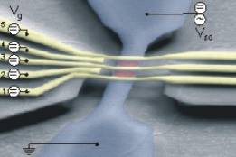
Figure 1. Free standing phonon cavity with integrated quantum dots and additional gate electrodes [3].
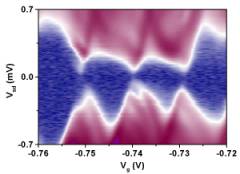
Figure 2. Coulomb blockade in a suspended quantum dot [3].
- "Integrating suspended quantum dot circuits for applications in nanomechanics", J. Kirschbaum, E. M. Höhberger, R. H. Blick, W. Wegscheider, and M. Bichler, Appl. Phys. Lett. 81, 280 (2002).
- "Single-Electron-Phonon Interaction in a Suspended Quantum Dot Phonon Cavity", E. M. Weig, R. H. Blick, T. Brandes, J. Kirschbaum, W. Wegscheider, M. Bichler, and J. P. Kotthaus, Phys. Rev. Lett. 92 (4), 046804 (2004)
- "Electron–phonon interaction in freely suspended quantum dots", E. M. Höhberger, J. Kirschbaum, R. H. Blick, J. P. Kotthaus, and W. Wegscheider, Physica E 18, 99 (2003)
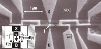
Primary thermometer formed by Coulomb islands in a suspended silicon nanowire
A. T. Tilke, L. Pescini, H. Lorenz, and R. H. Blick.
We realized thermometers in suspended highly n-doped silicon nanowires with lateral dimensions down to about 40 nm (see Fig. 1). Random dopant fluctuations in the suspended wires lead to the formation of multiple tunnel junctions, utilized for Coulomb blockade thermometry (see Figs. 2 & 3). In the low bias regime, we observe relaxation via discrete acoustic phonon modes to give a lower bound for the sensitivity [1].
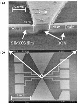
Figure 1. Suspended nanowire in a sideview (a) demonstrating complete suspension of the wire. The wire is integrated in a bow-tie antenna (b) for achieving maximal radiation coupling.
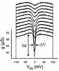
Figure 2. Temperature dependence of the conductance dip of the suspended nanowire caused by Coulomb blockade. The lowest trace is taken at 1.5 K and the upper most at 16.5 K.
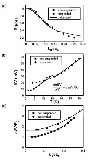
Figure 3. (a) Temperature dependence of the normalized amplitude of the conductance dip for the suspended and the non suspended wire. Also shown (solid line) is the calculated amplitude (b). Temperature dependence of the peak width (FWHM) dV of the conductance dip for the suspended and the nonsuspended wire. The slopes of the curves for high temperatures are almost identical. (c). Normalized dV as a function of temperature normalized to the effective temperature T / Teff = kB T / EC.
- A. T. Tilke, L. Pescini, H. Lorenz, and R. H. Blick: "Fabrication and transport characterization of a primary thermometer formed by Coulomb islands in a suspended silicon nanowire " Appl. Phys. Lett. 82, 3773 (2003).
Quantum interference in a one-dimensional silicon nanowire
A. T. Tilke, F. C. Simmel, H. Lorenz, R. H. Blick, and J. P. Kotthaus.
We studied the electronic transport within a lithographically defined silicon nanowire for zero and finite bias. The 10-nm wide and 500-nm long nanowires have been fabricated by advanced electron-beam lithographic techniques (see Fig. 1). Transport experiments reveal clear quantum size effects in the conduction through the wire. Energy quantization within the wire leads to a shift in conduction threshold (see Fig. 2). Quantum interference effects cause an oscillatory pattern in the conductance (see Fig. 3). At low source-drain bias, transport is dominated by shallow tunneling barriers. At higher bias, additional nanowire modes are found to contribute to the conductance [1].
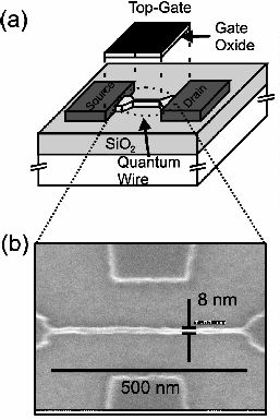
Figure 1. Sketch of the SOI nanowire: a metallic top gate is separated from the silicon quantum wire by a 55 nm silicon oxide. SEM micrograph of the nanowire defined in Calixarene with a width below 10 nm and a length of 500 nm.
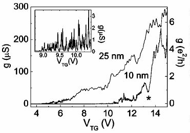
Figure 2. Top gate voltage dependence of the conductance of a 25 nm wide and a 10 nm wide silicon nanowire. The conductance in the narrow wire starts to rise at much higher gate voltage values than in the wide wire. This offset is due to the lateral energy quantization in the narrow wire. The asterisk marks a gate voltage value above which a strong increase in conductance can be noticed. This threshold behavior is caused by shallow tunnel barriers at the wire openings or within the wire. Inset: Magnified view of the conductance trace for the 10 nm wire between VTG = 8.5 and 10.5 V. The first resonances appear at VTG = 8.9 V which is taken as the onset gate voltage. The conductance peaks in this region remind of Coulomb blockade resonances. The mean spacing between adjacent conductance peaks corresponds roughly to the charging energy for the whole wire.
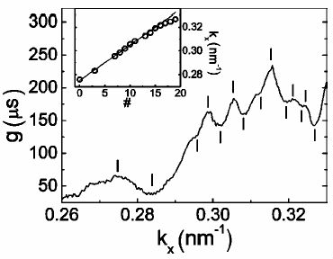
Figure 3. Resonant structure in the conductance of the narrow wire. Here the conductance is plotted as a function of the longitudinal wave number kx of the electrons along the transport direction. The maxima and minima are marked with vertical bars. In the inset, the positions of these extrema are plotted against their position number starting arbitrarily at 0 for the feature with the lowest kx value. The maxima and minima are well fit by a straight line corresponding to a resonant length which is roughly the wire length.
- A. T. Tilke, F. C. Simmel, H. Lorenz, R. H. Blick, and J. P. Kotthaus "Quantum interference in a one-dimensional silicon nanowire" Phys. Rev. B 68, 075311 (2003).
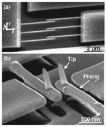
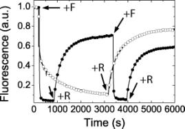
SAM-assisted assembly of carbon nanotubes on gold electrodes
Christian J.-F. Dupraz, Udo Beierlein, and J.P. Kotthaus.
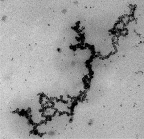
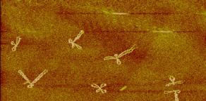
An attempt was made to decrease the contact resistance of CNT placed on top of a pair of gold electrodes. Instead of assembling the CNT`s on a substrate and depositing gold contacts afterwards, the electrodes were first optically defined. Similar to the attachment of DNA on gold [1], a monolayer of cysteamine was formed on the surface. The pretreated hydrophobic CNT-material, that is negatively charged favourably sticks to the now hydrophilic positively charged goldsurface. AFM-pictures (Fig. 1) show rather than bridging the contacts freely suspended the nanotubes prefer to adhere to the substrate. This could be due to vdW-interaction. Both types of nanotubes (MWNT and SWNT) are deposited and studied in their electrical transport properties. In both cases at 4.2 K the conduction is in the Coulomb blockade regime. Coulomb diamonds are visible, in the case of SWNT excited states are apparent (Fig. 2). The sharpness of the features in the diamonds of the SWNT, in contrast to measurements from MWNT, results from a further reduced size of the coulomb blockade islands. The room-temperature resistance of the MWNT-devices lies normally between 10 kOhm and several 100 kOhm, while the resistance of the SWNT reaches up to MOhm. The role of the cysteamine-molecules need not be a better coupling of the nanotube to the electrode, but could result in a cleaning of the goldsurface from adsorbates.
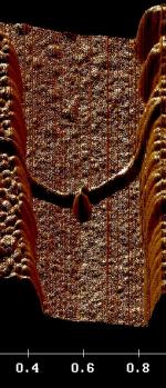
Figure 1. AFM-Picture of a MWNT lying over the contacts (scale-unit µm)
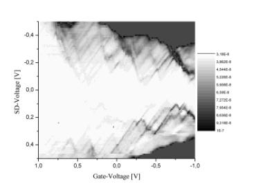
Figure 2. Conductance [S] of a SWNT at 4.2 K, excited states are visible
- G. Maubach, A. Csáki, D. Born and W. Fritzsche. Nanotechnology 14, 546-550 (2003)
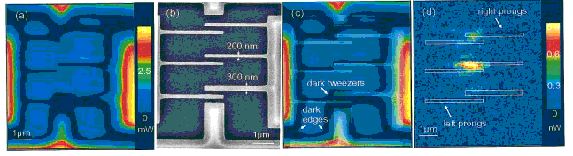
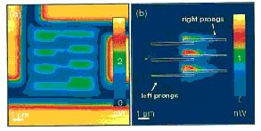
Nanostructures for testing molecular wires
Michael Lambacher, Christian J.-F. Dupraz, Udo Beierlein and Jörg P. Kotthaus, in collaboration with Philip Andres and Ulrich S. Schubert.
In order to continue the miniaturization of electronic elements to the nanometer scale, perhaps even to the molecular scale, researchers are investigating several alternatives to the transistor for ultra-dense circuitry. Many of these advances have been made possible by using the self-assembly of molecules on microfabricated semiconductor and/or metallic structures. In order to measure the electronic transport properties of self-assembled mono- and multilayers of thiol- and isocyanide-terminated molecules, we developed three different contact geometries [1]. E.g., pairs of gold electrodes with contact distances of a few nanometers can be fabricated by using a thin Al2O3 layer as a spacer between the electrodes. This can be achieved by optical and electron beam lithography and subsequent evaporation of gold, Al2O3 and gold (Fig. 1). Single layers of molecules or multilayers can then be inserted between the contacts where the oxide was partly removed in a wet etch process.
With all of these techniques, we observe peaks in the conductance versus source-drain-voltage curves which could arise from coherent transport through the molecular orbitals or from the coupling to the vibrational modes of the molecules (Fig. 2).
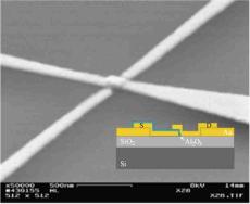
Figure 1. SEM image of an electrode pair and two gate electrodes for conductance measurements of self-assembled mono- and multilayers.
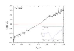
Figure 2. Current as a function of source-drain voltage before (red) and after insertion of chains of 1,4 phenylenediisocyanide (black curve) at 290 K. Inset: Conductance vs. VSD at low temperature.
- Dupraz C.J.-F., Beierlein U., Kotthaus J.P., CHEMPHYSCHEM 4 (11), 1247, 2003.
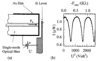
Low-temperature, in situ tunable, uniaxial stress measurements in Semiconductors using a piezoelectric actuator
M. Shayegan, K. Karrai, and S. Manus, in cooperation with Y. P. Shkolnikov, K. Vakili, and E. P. De Poortere.
We demonstrated the use of a piezoelectric actuator to apply, at low temperatures, uniaxial stress in the plane of a two-dimensional electron system confined to a modulation-doped AlAs quantum well. Via the application of stress, which can be tuned in situ and continuously, we control the energies and occupations of the conduction-band minima and the electronic properties of the electron system. We also reported measurements of the longitudinal and transverse strain versus bias for the actuator at 4.2 K, both of which are nearly linear and shows very little hysteresis with the applied bias.
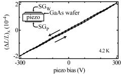
Figure 1. Longitudinal strain vs piezo bias, measured at 4.2 K, with a strain gauge (SGW) glued on top of a 0.1 mm thick GaAs wafer that is in turn glued to the piezo Inset: Data are shown for up and down directions of piezo bias sweeps.
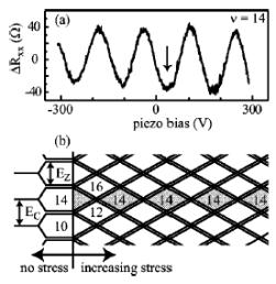
Figure 2. (a) Change in resistance of an AlAs 2D electron system at filling factor n=14 (B=1.78 T) and at T=50 mK as a function of bias applied to the piezo rod. The vertical arrow indicates the position of zero stress. (b) Schematic energy level diagram for the AlAs 2D electrons in the presence of a fixed B, ignoring B-induced enhancement of valley splitting.
- M. Shayegan, K. Karrai, Y. P. Shkolnikov, K. Vakili, E. P. De Poortere and S. Manus, “Low-temperature, in situ tunable, uniaxial stress measurements in Semiconductors using a piezoelectric actuator”, Appl. Phys. Lett., 83, 5235 (2003).
Optics with nanostructures
Excitons in self-assembled quantum dots constitute another atomic-like solid state system ideally suited to study quantum properties and attractive for storing qubits. Here we combine our know-how of filling quantum dots with well-defined exciton and electron occupation with the expertise developed to perform a range of luminescence and absorption experiments on individual quantum dots. Electron-occupation dependent fine-structure of the luminescence nicely reflects the quantum nature of the charged excitonic states as well as their interaction with a nearby two-dimensional electron system. Absorption spectroscopy on individual quantum dots enabled by Stark-shift modulation spectroscopy yields quantitative insight lifetime broadening and oscillator strength of excitonic transitions and charge-tunable exchange coupling. In an international collaboration our experimental studies are complemented by theoretical efforts aiming to understand the interaction between excitons in the dot and a nearby Fermi sea. We also develop methods to trap long-living spatially indirect excitons in a double quantum well into defined lateral potential geometries ranging from 1D stripes to fully confining excitonic traps. The experiments aim at a better understanding of the temporal and spatial dynamics of such long-living excitons. In similar devices containing a single quantum well we have utilized the reversible spatial separation of optically generated electron-hole pairs via two-dimensional electrostatic potentials to create a photonic camera. This enables us to store and modify whole pictures for times up to seconds before being reemitted as excitonic luminescence.
Fine structure of highly charged excitons in semiconductor quantum dots
B. Urbaszek, and K. Karrai, in cooperation with R.J. Warburton, B. Gerardot, P. M. Petroff, and J. M. Garcia.
An exciton in a symmetric semiconductor quantum dot has two possible states, one dark and one bright, split in energy by the electron-hole exchange interaction. We demonstrate that for a doubly charged exciton, there are also two states split by the electron-hole exchange, but both states are now bright. We also uncover a fine structure in the emission from the triply charged exciton. By measuring these splittings, and also those from the singly charged and doubly charged biexcitons, all on the same quantum dot, we show how the various electron-hole exchange energies can be measured without having to break the symmetry of the dot.
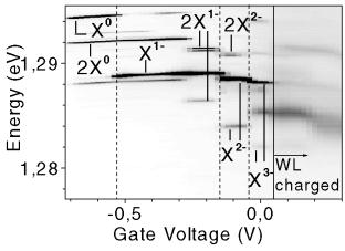
Figure 1. Gray-scale plot of the photoluminescence versus gate voltage for a single dot from sample A at 4.2 K. White corresponds to 0 counts, black to 4000 counts on the detector. The excitons are labeled with X standing for exciton, 2X for biexciton, with excess charge as the suffix. Dotted lines mark charging events. The unlabeled emission at 1.288 eV is related to 2X0, but its exact origin is presently unknown. The power of the 850 nm laser was chosen so that the biexciton features are clearly visible. Above a voltage of about 0.05 V, the wetting layer (WL) loads with electrons.
- B. Urbaszek, R.J. Warburton, K. Karrai, B. Gerardot, P. M. Petroff, and J. M. Garcia: “Fine structure of highly charged excitons in semiconductor quantum dots”, Physical Review Letters 90, 247403-1 (2003).
Stark-shift modulation absorption spectroscopy of single quantum dots
B. Alèn, F. Bickel, K. Karrai, in cooperation with R. J. Warburton, and P. M. Petroff.
Excitonic interband optical transitions within single InAs self-assembled quantum dots have been directly observed in a transmission experiment at 4.2 K. Using Stark shift, the excitonic energy levels of a single quantum dot are tuned into resonance with a narrow-band laser line. The Stark shift is also modulated at low frequencies. Relative changes in transmission can be detected this way down to one part per million. The oscillator strength as well the homogeneous linewidth of the transition is obtained.
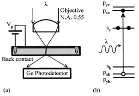
Figure 1. (a) Transmission measurement schematics (to scale). The Ge detector is placed directly behind the sample at 4.2 K. (b) The optical absorption creates an exciton with its electron and hole in a p level of the InAs quantum dot. Here, we illustrate two electrons filling the s shell.
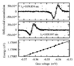
Figure 2. Top: Differential transmission obtained by Stark-shift modulation of the excitonic dot absorption. The multiple lines originate from different excitonic transitions in several dots. Bottom: Modulated excitonic absorption line from a single optical transition in a single quantum dot.
- B. Alèn, F. Bickel, K. Karrai, R. J. Warburton and P. M. Petroff, „Stark-shift modulation absorption spectroscopy of single quantum dots”, Appl. Phys. Lett 83, 2325 (2003).
Kondo excitons in self assembled quantum dots
K. Karrai, in cooperation with R. J. Warburton, and A. O. Govorov.
We describe excitons in quantum dots by allowing for an interaction with a Fermi sea of electrons. We argue that these excitons can be realized very simply with self-assembled quantum dots, using the wetting layer as host for the Fermi sea. We show that a tunnel hybridization of a charged exciton with the Fermi sea leads to two striking effects in the optical spectra. First, the photoluminescence lines become strongly dependent on the vertical bias. Second, if the exciton spin is nonzero, the Kondo effect leads to peculiar photoluminescence line shapes with a linewidth determined by the Kondo temperature.
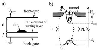
Figure 1. (a) Schematic of the heterostructure with a quantum dot embedded between front and back gates; d<<l. (b) The band diagram of a quantum dot and associated wetting layer showing also the energies typical to self-assembled quantum dots.
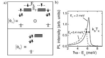
Figure 2. Contributions to the initial state (b) Calculated emission spectrum of the X2- exciton with the triplet final state configuration;
- A. O. Govorov, K. Karrai, and R. J. Warburton, “Kondo excitons in self assembled quantum dots”, Phys. Rev. B67, 241307R (2003).
Dynamics of excitons in coupled quantum wells
Andreas Gärtner, and Jörg P. Kotthaus, in cooperation with Dieter Schuh and Max Bichler.
The experiments to learn more about motion and interaction of excitons are carried out in semiconductor heterostructures at low temperatures (4K). The heterostructures contain two quantum wells (QWs), which are coupled by a thin tunneling barrier. Patterned gate structures applied to the samples allow impressing electrical fields on the QWs.
Via the electrical field applied perpendicularly to the QWs, we can prolongate the lifetime of excitons by orders of magnitude to 250 ns (see Fig.1). The long life time of these so-called spatially indirect excitons allows us to study excitonic drift properties. Utilizing the Quantum Confined Stark Effect (QCSE) of excitons, a lateral potential landscape for excitons Uexc is created in the QW plane [1,2]. This we use to externally control the drift of the electrically neutral excitons. The black curve in Fig.3 shows maxima and minima of the emitted PL in an excitonic potential with a lateral periodicity of 4µm created by an interdigitated gate structure. Reversing the excitonic potential by swapping the gate voltages, the PL replies by moving half a period (red curve). Reversing the voltages again, the spatial PL emission is shifted again to its initial distribution (green curve).
Specially designed gate patterns allow a wide range of lateral modulations of Uexc and, ultimately, the creation of artificial traps confining long-living indirect excitons in all spatial dimensions.
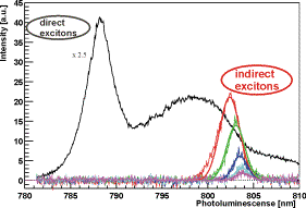
Figure 1. Spectrally resolving the PL emitted by the coupled QWs at 4K allows to distinguish between short-living direct excitons (black curve, measured during 680nm-laser illumination) and long-living indirect excitons (colored curves, taken at various time intervals after shutting off the excitation laser).
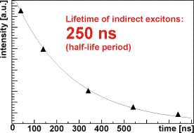
Figure 2. In this experiment, the indirect excitons show a lifetime of 250ns, which is deduced from the exponential decrease of their PL intensity.
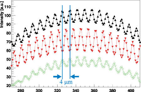
Figure 3. Changing the modulation of the excitonic potential (different curves) causes variations in the lateral distribution of the emitted PL.
- S. Zimmermann et al., Phys. Rev. B 56, 13414 (1997)
- S. Zimmermann et al., Appl. Phys. Lett. 73, 154 (1998)
Quantum well photography
Jan Krauß, Achim Wixforth, and Jörg P. Kotthaus, in cooperation with Micah Hanson, Dan C. Driscoll, Arthur C. Gossard, Dieter Schuh, and Max Bichler.
We have realized the capture of optical images in the plane of a semiconductor quantum well and the subsequent re-emission of this image in form of a two-dimensional photon flux. Spatially resolved storage of photonic signals in an electrostatically induced two-dimensional potential landscape in the plane of the quantum well is employed to imprint optical images in form of trapped photogenerated charges into the solid. The two-dimensional potential modulation leads to very long storage times by a deliberate spatial separation of photogenerated electron-hole pairs. Once the potential modulation is lifted, radiative electron-hole recombination restores the initial optical pattern and the photographed image is released in a flash of light as demonstrated in Fig. 1
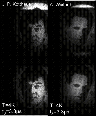
Figure 1: Images projected onto a quantum well laterally modulated by a two-dimenional electrostrostatically generated potential of 2mm x 4mm period (top) and released as light via excitonic recombination after a storage time of 3.8 msec (bottom). The active device area is 400mm x 500mm containing 200x125 pixels.