

E. Nanodevices and Bio-templated Nanostructures
Science and technology on the scale of a nanometer -one billionth of a meter- is revolutionary. Nanotechnology refers to the ability to manipulate individual atoms and molecules, making it possible to build machines on the scale of human cells or create materials and structures from the bottom up or from the top down, building in desired properties.
Applications of nanotechnology include:
- Materials with desirable properties such as high strength, chemical sensing or optical switching designed in from the start.
- Information technology by quantum computing and computer chips that store trillions of bits of information on a pin-head device.
- Medical applications with improved drug and gene delivery, biocompatible materials for implants and nanoscale sensors for detection of disease.
The goals of our nanoscale research and engineering are:
- Biosystems at the nanoscale - the relationship among chemical composition, shape and function.
- Nanoscale structures, novel phenomena and quantum control - how to overcome existing limits to miniaturization.
- Device and system architecture - integrating nanoscale devices into measurement and control assemblies.
We investigate realizations of devices fabricated in silicon-on-insulator (SOI)-films, e.g. electrically driven nanotweezers, which allow a specific manipulation of particles with sizes in the range of some 10 nm.
Other topics of our nanodevice research combine the fixing and manipulation of DNA on microstructured surfaces.
Also, we have investigated the mechanical properties of nanometer sized diamond-like atomic-force microscope tips.
Our research with nanodevices splits in the following projects:
-
Optical Investigation of Nanotweezers' Deflections
Christine Meyer, Heribert Lorenz, Khaled Karraï, and Jörg P. Kotthaus. -
Manipulation of DNA on microstructured surfaces
Stefan Beyer, Wendy Huynh, Friedrich Simmel -
Mechanical properties of high-aspect-ratio atomic-force microscope tips
Armin Kriele and Heribert Lorenz in cooperation with Gerit Jänchen and Pepter Hoffmann.
Optical Investigation of Nanotweezers' Deflections
Christine Meyer, Heribert Lorenz, Khaled Karraï, and Jörg P. Kotthaus.
Nanotweezers, the nanoscopic analogs of normal laboratory tweezers, could be very helpful tools for rearrangements of nanometer-sized objects. We use electron beam lithography and diverse etching techniques to fabricate the tweezers out of SOI material. Electron beam deposited tips are grown on top of the silicon prongs. A scanning electron micrograph of such a freely suspended tweezers structure is shown in fig. 1. They are to be actuated electrostatically.
Having built the nano-electromechanical structure, it is necessary to prove its functionality. For this purpose, an optical method was investigated. Images of the tweezers structures were taken by scanning confocal microscopy while the prongs were electrostatically deflected under a low frequency ac voltage. The images clearly resolve the actuating parts of the tweezers.
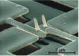
Figure 1. The nanotweezers consist of two freely suspended prongs, each being 3 μm long, 200 nm wide and 150 nm thick, with electron beam deposited tips grown on top of them.
Manipulation of DNA on microstructured surfaces
Stefan Beyer, Wendy Huynh, Friedrich Simmel
Due to its extraordinary molecular recognition properties DNA is ideally suited for molecular self-assembly. DNA has already been used for the construction of complicated supramolecular structures such as polyhedra or two-dimensional crystals. Quite recently, DNA hybridization has even been exploited to drive nanoscale motion. In this project we aim at using DNA as a template for the assembly of nanoscale electronic circuits. One crucial step towards this goal is the functionalization of electrodes with DNA strands. These DNA "sticky labels" may be used to molecularly address specific electrodes during the self-assembly process. Currently, we explore several techniques to manipulate and position individual DNA strands on microstructured surfaces. Among these are electrostatic trapping and stretching of DNA (fig. 1) and also molecular combing techniques (fig. 2).
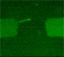
Figure 1. Fluorescence microscopic image taken during electrostatic stretching of fluorescently labelled λ-DNA between gold microelectrodes on glass. The gap between the electrodes is about 12 μm wide. The DNA strand is the bright beam emanating from the left electrode.
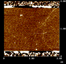
Figure 2. AFM image of DNA bridging the gap between two gold electrodes on silicon. The sample has been prepared using molecular combing techniques. The width of the gap between the electrodes is below 2 μm.
Mechanical properties of high-aspect-ratio atomic-force microscope tips
Armin Kriele and Heribert Lorenz in cooperation with Gerit Jänchen and Pepter Hoffmann.
Focused-electron-beam-deposited carbon atomic-force microscope tips were characterized using flexural vibrations excited with piezoelectric transducers and observed directly inside a scanning electron microscope. Frequencies in the high-MHz range were measured and the elastic modulus was estimated to be 0.54 ± 0.16 TPa.
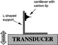
Figure 1. Dynamic method used to determine elastic properties of carbon tips. The method is based on the measurement of the vibrating tip's mechanical resonance. Tip vibration is excited by an ultrasonic transducer. Longitudinal transducer movements (in the figure, up-down) excite flexural tip vibrations through the L-shaped support. The resonance of the support can be clearly distinguished from the tip resonance.
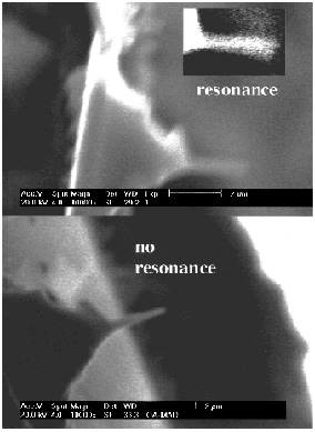
Figure 2. SEM micrographs showing mechanical resonance of the 2.4 micron carbon supertip at 46.9 MHz excitation frequency (above, inset: zoom of carbon tip) and the same tip not in resonance (below). Applying Timoshenko formula the calculated Young's modulus is 0.67 TPa with an assumed hard core tip radius of 50 nm and a chosen density of 3.0 g/cm
- G. Jänchen, P. Hoffmann, A. Kriele, H. Lorenz, A. J. Kulik, and G. Dietler, Appl. Phys. Lett. 80, 4623-4625 (2002)