

C. Static and Dynamic Lateral Superlattices
The here studied Surface Acoustic Waves (SAW) are the nanometer analogon of earthquakes. Devices based on such SAWs are usually used for radio frequency communication, acting as RF filter elements. SAWs are easily excited on piezoelectric solids. Such materials deform, if an electric field is applied to them. Rapid changes of such electric fields generated with an appropriate transducer are efficiently converted into a 'nanoquake on a chip'. Our experiments presently cover the frequency range between 100 MHz and 6 GHz, corresponding to surface acoustic wavelengths between 30 and 500 nm, respectively.
The electric fields of the wave can couple to the mobile carriers within a semiconductor structure and modify its electronic properties. By measuring the attenuation of the wave and the renormalization of the sound velocity we can, for instance, extract information on the dynamic conductivity of the electron system. We also investigate the possibility to use a SAW for a dynamical lateral potential modulation and we study the influence of a SAW onto the optical properties of an electron system. Static superlattices can be used as another method to influence the optical properties of a semiconductor sample.
Also, additional mass loading on the substrate surface leads to damping of the SAW. By fictionalizing the surface of the device under test, this effect can be used for chemical sensor applications. To achieve spatial resolution, a special transducer design is introduced. Recently, we demonstrated that the mechanical interaction between SAWs and fluids can be exploited to realize new micro- and nanofluidic devices.
The SAW - related research in 2002 was structured in the following topics:
-
Mikro- and nanofluidic on piezoelectric susbtrates
C. J. Strobl and A. Wixforth
in cooperation with Advalytix AG and University of Augsburg. -
Imaging of the Interaction between Surface Acoustic Waves and Excitons
Hans-Jörg Kutschera, Christoph Bödefeld, and Achim Wixforth. -
Linear and Nonlinear Acoustoelectric and Acoustophotoelectric Effects
Hans-Jörg Kutschera, Achim Wixforth, Alexander V. Kalameitsev, and Alexander O. Govorov,
in cooperation with Dan C. Driscoll, Micah Hanson, Christoph Kadow, Art C. Gossard. -
Surface Acoustic Wave Studies for Chemical Sensors and Optical Imaging Devices
Alexander Möller, Hans-Jörg Kutschera, and Achim Wixforth -
Charge Carriers in Static Lateral Superlattices
Jan Krauß, Alexander V. Kalameitsev, Alexander O. Govorov, Achim Wixforth, and Jörg P. Kotthaus
in cooperation with Dan C. Driscoll, Micah Hanson, Art C. Gossard, and Dieter Schuh, Max Bichler, Werner Wegscheider.
Mikro- and nanofluidic on piezoelectric susbtrates
C. J. Strobl and A. Wixforth
in cooperation with Advalytix AG and University of Augsburg.
The handling of liquids in the submilliliter scale is usually governed by crucial difficulties. The use of a surface acoustic wave device in a Rayleigh wave mode as a microfluidic pump promises a lot of advantages. SAW devices as an approach towards a lab on a chip are demonstrated for various applications. In biology, the sorting of particles or molecules by electric fields is one of most important experiments. To investigate the usage of electric fields in a microfluidic system it is necessary to reduce the mechanical influence to the liquid leading to the effect of acoustic streaming. Such a reduction is for instance reached by using a thin liquid layer. The reduction of the layer thickness causes a deceleration of the fluid flow. If the thickness of the liquid layer is comparable to the SAW wavelength, we were able to observe a SAW induced alignment of Carbon Nanotubes (NT) (s. fig. 1). This alignment is caused by the influence of the electric fields of the SAW to the NT's.
The effect of acoustic streaming is also observable on substrates with a shear wave mode. Furthermore, shear waves can be used as a sensor in liquids. This opens the possibility to detect the conductivity of, e.g., a salt solution during a mixing experiment. An important consequence is, that here is a good possibility for the combination of actuation and sensors.
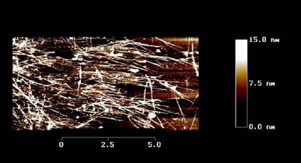
Figure 1. AFM image of NT's on lithiumniobate after they was given an orientation. The SAW propagated from left to the right side. All tubes with orientation are in contact to the surface. There are still tubes without orientation but in contrast to the orientated NT's they have no contact to the substrate. The scale beneath the AFM image is in micrometer.
Imaging of the Interaction of Surface Acoustic Waves with Excitons
Christoph Bödefeld, Hans-Jörg Kutschera, and Achim Wixforth.
Using an intensified CCD in combination with a microscopic setup, we are able to investigate the interaction between a surface acoustic wave (SAW) and photogenerated excitons in semiconductor heterostructures. Due the electric fields accompanying the SAW on a piezoelectric substrate, like GaAs, the excitons get ionised an the photoluminescence (PL) is quenched [1]. This effect can be applied e.g. to record the propagation of a SAW. In Fig 2. we see an image of an homogenously illuminated delayline under the influence of a short SAW pulse. As one can easily see, the PL is modified in two ways: Wherever the SAW is strong enough the PL is decreased. Whereas right in front of the SAW pulse the PL is increased. The first effect is due to the just discussed quenching of the PL, the second is based on an increased emission rate of surface states [2]. The time evolution of this pulse is illustrated in Fig. 3. Here the image is integrated perpendicular to the SAW propagation and recorded at different times after the SAW is launched. The optical signal corresponds to the electrical transmission and reflection signal of the SAW delayline.
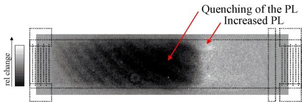
Figure 2. Image of a surface acoustic wave propagating on a semiconductor heterostructure, 600 ns after emission from the left interdigital transducer. The photoluminescence induced from a laser is strongly modulated by the SAW.
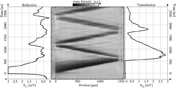
Figure 3. Time evolution of a SAW
- C. Rocke et al., Phys. Rev. Lett. 78, 4099 (1997).
- D. Janes et al., J. Appl. Phys. 67, 6315 (1990).
Linear and Nonlinear Acoustoelectric and Acoustophotoelectric Effects
Hans-Jörg Kutschera, Achim Wixforth, Alexander V. Kalameitsev, and Alexander O. Govorov,
in cooperation with Dan C. Driscoll, Micah Hanson, Christoph Kadow, Art C. Gossard.
We study experimentally the interaction of intense surface acoustic waves with an electron and an electron-hole plasma of a quantum well. The experiments performed on hybrid semiconductor-piezocrystal structures (Fig. 4) exhibit strong nonlinear acoustoelectric and acoustophotoelectric effects due to the formation of moving electron and electron-hole wires, respectively. It was shown theoretically that the nonlinear interaction of a SAW with a photo-generated electron-hole plasma qualitatively differs from the case of an unipolar electron system [1]. For low temperatures in the regime when the intense SAW forms moving quantum wires or quantum dots we expect a novel quantum acoustic phenomenon: self-induced acoustic transparency [2].
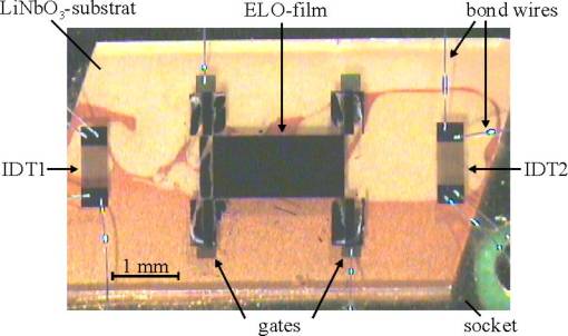
Figure 4. Typical sample to study nonlinear effects. The hybrid structure consists of a strong piezoelectric substrate (LiNbO3) with a submicrometer thin semiconductor heterostructure on top. At the left and right, one can also see the two interdigital transducers IDT1 and IDT2 of the SAW delayline.
- A. O. Govorov, A. V. Kalameitsev, M. Rotter, A. Wixforth, J. P. Kotthaus, K.-H. Hoffmann, N. Botkin, Phys. Rev. B 62, 2659 (2000).
- A. O. Govorov, A. V. Kalameitsev, V. M. Kovalev, H.-J. Kutschera, and A. Wixforth, Phys. Rev. Lett. 87, 226803 (2001).
Surface Acoustic Wave Studies for Chemical Sensors and Optical Imaging Devices
Alexander Müller, Hans-Jörg Kutschera, and Achim Wixforth
Photogenerated charge carriers and/or additional mass loading on the substrate surface changes the SAW's transmission signal. This can be used for optical or chemical sensor applications. To achieve spatial resolution, we use so called fan shaped transducers (see inset of fig.5). Because of their varying finger period, it is possible to launch only a narrow SAW path along the delay line. The position of this path can be determined by the driving frequency.
This allows us e.g. to spatially resolve chemical adsorbants. A 200 nm thick Apiezon W layer serves as active layer of our first chemical sensor. Fig.5 shows the sensitivity to trichlorethylene which is a good solvent for Apiezon W. The SAW's phase signal of an acoustic path crossing the Apiezon W layer shifts relative to the phase of the reference SAW while the carrier gas is seeded with trichlorethylen. A much smaller relative shift occurs for an acoustic path crossing the layer that consists of photo resist.
Also an optical imaging device has been realized, which includes a 350 nm thick semiconducting epitaxial-lift-off (ELO) layer on top of a strong piezoelectric substrate (see inset fig.6). The transmission properties of the probe SAW is modified under the presence of charge carriers, if there is an intense perpendicular SAW. We can use this nonlinear interaction to resolve the spatial distribution of photogenerated charges. Therefore we are able to reconstruct simple patterns of an illuminated area on the semiconductor (fig. 6) [1, 2].
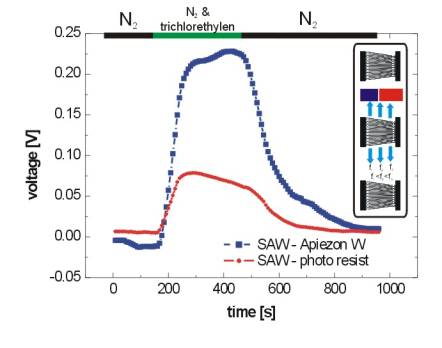
Figure 5. Phase shift of the sensor delay line relative to the reference delay line. The sensor delay line consists of an Apiezon W and a photo resist layer along the SAW path.
Figure 6. The transmission signal of a SAW with frequency fprobe changes if a perpendicular SAW with frequency fpump is intense enough and charge carriers are present. The change in phase (blue) or amplitude (red) of the probe SAW is shown for different frequencies of the SAW. The pattern of the illuminated area is sketched by the red dots and lines.
- A.C. Müller, H.-J. Kutschera, and A. Wixforth, Spatially Resolved Surface Acoustic Wave Studies For Image Processing And Chemical Sensors, EFTF 2002 St. Petersburg, in press.
- A.C. Müller, H.-J. Kutschera, and A. Wixforth, Spatially Resolved Surface Acoustic Wave Studies For Image Processing, IEEE Ultrasonic Symposium 2002, in press.
Charge Carriers in Static Lateral Superlattices
Jan Krauß, Alexander V. Kalameitsev, Alexander O. Govorov, Achim Wixforth, and Jörg P. Kotthaus
in cooperation with Dan C. Driscoll, Micah Hanson, Art C. Gossard, and Dieter Schuh, Max Bichler, Werner Wegscheider.
Lateral potential modulation in semiconductor heterostructures is realised by voltages applied to interdigitated metal electrodes on top of the structure. The depth of the modulation can therefore be tuned at will.
By switching the potential form type-II-modulation to flat-band, spatially separated electron-hole pairs can be triggered to recombine radiatively after a certain storage time, exceeding the radiative lifetime in these structures by orders of magnitude [1]. This "photonic memory" was used to visualise carrier dynamics by taking luminescence images which directly correspond to the carrier (hole) distribution. Taking several images at different storage times allows us to record "Movies" of the charge evolution. In Fig. 7, such a "snapshot" is shown for a regular interdigitated electrode [2]: Carrier motion is possible only along the stripe-like electrodes (horizontally). Fig. 9 however shows a comparable image in a more complex structure [3]: The electrodes have a wider area, where luminescence - thus carriers- accumulate. The geometrical shape of the electrodes strongly influences the luminescence pattern, indicating that strain induced in the semiconductor structure due to the metal on top is playing a crucial role in these systems.
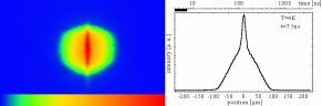
Figure 7. Luminescence distribution in a regular structure (left) and cross section along the electrodes together with the respective delay time (right), corresponding directly to the distribution of the photogenerated holes [2] (see the animated gif ). Due to the sample structure, motion is only possible horizontally. The colour coding of the intensity scale below is ranging from blue (dark) to red (bright).
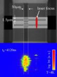
Figure 8. Photopgraph and sketch (not to scale) of the electrode-structure (top) and corresponding luminescence image after a storage time of 4120ns (bottom). The luminescence accumulates in the region of wide electrode stripes.
- S. Zimmermann, A. Wixforth, J. P. Kotthaus, W. Wegscheider, and M. Bichler, "A Semiconductor Based Photonic Memory Cell", Science 283, 1292-1295 (1999).
- J. Krauß, A. Wixforth, A. V. Kalameitsev, A. O. Govorov, W. Wegscheider, and J. P. Kotthaus, "Nonlinear Charge Spreading Visualized in Voltage-Controlled Lateral Superlattices", Phys. Rev. Lett. 88, 036803 (2002).
- J. Krauß, A. Wixforth, J. P. Kotthaus, D. Schuh, and M. Bichler in Proceedings of the ICPS-26, Edinburgh, to be published