

A. Electronic Properties of Nanostructures
Non-diffusive electronic transport phenomena which display characteristics of semiconductor nanostructures are investigated at low temperatures in a variety of devices, mostly fabricated out of layered semiconductor structures employing the high resolution electron beam lithography in our clean room. Following a proposal by R. Fleischmann, we study the transport mechanisms which cause non-linear ballistic rectification in asymmetric cross-junctions carved out of a two-dimensional electron gas (2DEG) on GaAs. We also investigate phase coherent transport at lowest temperatures (<1K) by embedding two electrostatically defined quantum dots in an Aharonov-Bohm ring. In similar quantum dots with suitably chosen spin configuration in the electronic ground state we observe spin blockade of single electron transport. We are able to fabricate ultra small quantum dots and quantum wires out of layered silicon-on-insulator systems which exhibit single electron transport phenomena at comparably high temperatures. Furthermore, we carried out conductance measurements through quantum wires in bridge-like suspended carbon nanotubes and self-assembled monolayers of organic molecules. A newly developed low temperature scanning probe instrument enables us to measure extremely small electrostatic forces and to image potential landscapes and individual charges close to surfaces. Further details can be found via the links below.
-
Probing and Controlling the Bonds of an Artificial Molecule
A. W. Holleitner, A. Hüttel, R. H. Blick, and J. P. Kotthaus
in cooperation with K. Eberl. -
Conductance measurements of self-assembled monolayers of 1,4-phenylene diisocyanide
Christian J.-F. Dupraz, Udo Beierlein, and Jörg P. Kotthaus -
Molecular Thermometry
Christian Schäflein, Udo Beierlein, and Jörg P. Kotthaus -
Tunable Ballistic Rectifier
Stefan de Haan, Axel Lorke, and Jörg P. Kotthaus
in cooperation with Max Bichler and Werner Wegscheider -
Observing nuclear spin polarization in a quantum dot
Andreas K. Hüttel, J. Weber, and Robert H,
in cooperation with Karl Neumaier and Karl Eberl. -
Single-electron effects in highly doped polysilicon nanowires
Armin Tilke, Robert H. Blick, Heribert Lorenz, and Jörg P. Kotthaus -
Electron-phonon interaction in suspended highly doped silicon nanowires
Armin Tilke, Laura Pescini, Heribert Lorenz, and Robert H. Blick -
Transport properties of freely suspended low-dimensional electron gases
Eva M. Höhberger, J. Kirschbaum, T. Krämer, and R. H. Blick
in cooperation with Max Bichler and Werner Wegscheider.
Probing and Controlling the Bonds of an Artificial Molecule
A. W. Holleitner, A. Hüttel, R. H. Blick, and J. P. Kotthaus,
in cooperation with K. Eberl.
We focus on coherent contact to molecular states of a double quantum dot in an AlGaAs/GaAs heterostructure where both dots are connected in parallel to source and drain reservoirs via quantum point contacts T1, T2, T3 and T4 (see Fig. 1(a)). Furthermore, the superposition of the dot wave functions is continuously controlled by a tunable inter-dot tunneling barrier TAB (see Fig. 1(a) and (b)). Cryogenic transport spectroscopy reveals that weak coupling of the quantum dots (containing 15 to 20 electrons each) to the reservoirs and an intermediate inter-dot coupling allow to coherently contact molecular states of the double quantum dot via correlated tunneling of two electrons [1]. Very distinct to prior work [2,3], this virtual process at resonance resolves sequences of molecular states simultaneously since no charging energy has to be paid in order to trace the quantum states. Fine tuning of all tunneling barriers allows well to distinguish between first order tunneling processes governed by orthodox Coulomb-theory (arrows in Fig. 2) and second order electron tunneling essential for the coherent probing described here (circle in Fig. 2). Temperature dependent measurements support the resemblance of the virtual two-electron process with correlated tunneling phenomena known from Kondo-physics where local spins are screened via virtual spin-flip processes. Via the electrostatic influence of top electrodes GA and GB (see Fig. 1(b)) we coherently trace the transition of an ionic quantum dot molecule to a covalent artificial molecule with fully delocalized electron wave functions [1]. In principle, our results can be used to prepare and probe entangled molecular states for future quantum information technology.
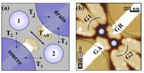
Figure 1. A. (a) Experimental outline (see ref. [1]): two quantum dots are coupled in parallel via tunneling barriers T1, T2, T3,T4 to source and drain. The inter-dot tunneling barrier TAB defines the superposition of the dot wave functions. (b) Atomic force micrograph of a real sample: voltages applied to gates GA and GB determine TAB, whereas to gates G1 and G2 shift the chemical potentials of each quantum dot. The contact regions of both dots (dashed lines) are patterned with an additional dielectric spacer in order to provide the parallel access [2,3].
Figure 2. While first order tunneling can be suppressed (white arrows), resonant co-tunneling of two electrons can be seen along lines in a typical phase diagram where an electron is delocalized over both dots (white circle) (see also ref. [1]).
- A. W. Holleitner, R. H. Blick, A. K. Huettel, K. Eberl, and J. P. Kotthaus, Science 297, 70 (2002).
- A. W. Holleitner, C. R. Decker, H. Qin, K. Eberl and R. H. Blick, Phys. Rev. Lett. 87, 256802 (2001).
- A. W. Holleitner, R. H. Blick, H. Qin, A. K. Hüttel, K. Eberl und J. P. Kotthaus, Physica E 12, 774 (2002).
Conductance measurements of self-assembled monolayers of 1,4-phenylene diisocyanide
Christian J.-F. Dupraz, Udo Beierleink, and Jörg P. Kotthaus
Electronic transport measurements were carried out in self-assembled monolayers of 1,4-phenylene diisocyanide using two different approaches: A single monolayer was sandwiched between two small gold contacts by use of nanolithographical and evaporation techniques (Fig 3.). The second technique involved a set of planar gold contacts with a separation of less than 10 nm between which self-assembled chains composed of 1,4-phenylene diisocyanide and Cobalt(II) ions were inserted (Fig. 4.). Conductance measurements at low temperature show discrete structures for both types of devices which are interpreted as arising from quantum transport through molecular ensembles.
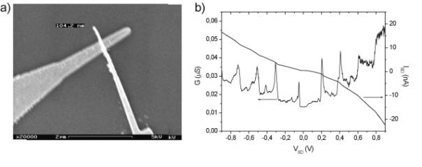
Figure 3. a) Crossed gold-contacts used for conductance measurements of self-assembled monolayers, b) conductance and current versus source-drain voltage of a self-assembled monolayer of 1,4-phenylene diisocyanide at 4.2 K.
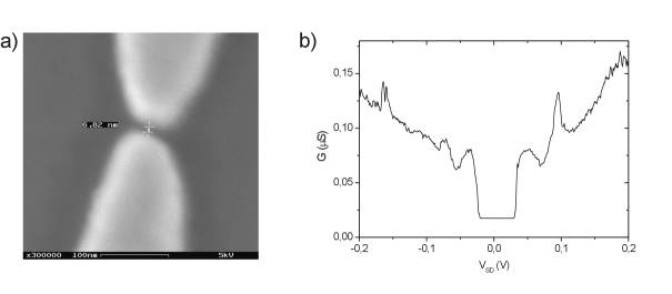
Figure 4. a) SEM image of the electrode gap of a of 1,4-phenylene diisocyanide/Cobalt(II) multilayer device (electrode distance: 7 nm), b) conductance as a function of source-drain voltage of such a device at 4.2 K.
Molecular Thermometry
Christian Schäflein, Udo Beierlein, and Jörg P. Kotthaus
A single-wall carbon nanotube (SWNT) is a single sheet of graphite rolled up into a cylinder. The minimum diameter of such a SWNT is less than 1 nanometer! If two or more sheets of graphite are rolled up into a cylinder we speak of multi-wall carbon nanotubes (MWNTs). By electrically contacting a suspended MWNT with lithographically defined metallic electrodes, we realized a primary thermometer with dimensions down to 4 nm in width. The electrically contacted nanotube can be understood as a series of quantum dots or tunnel junctions. The differential conductance of such a series of tunnel junctions displays a temperature dependent dip at zero bias [1]. Fig. 5 shows such a typical conductance dip of a suspended MWNT for different temperatures ranging from about 4 K to 24 K. Fig. 6 shows the linear relationship between FWHM of the conductance dip and the temperature for a suspended MWNT. Due to the small dimensions of the device and the high thermal conductivity of MWNTs, the estimated time constant of the suspended devices is with about 10-14 s extremely small [2, 3]. This allows ultra fast and sensitive temperature measurements.
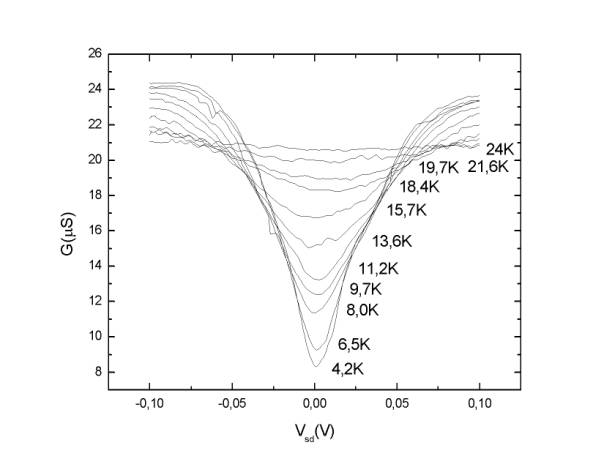
Figure 5. Temperature dependence of the conductance dip of a suspended MWNT.
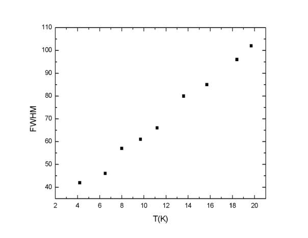
Figure 6. Temperature dependence of FWHM for a suspended MWNT.
- J. P. Pekola, K. P. Hirvi, J. P. Kauppinen, and M. A. Paalanen, Phys. Rev. Lett. 73, 2903 (1994)
- V. N. Popov, Phys. Rev. B 66, 153408 (2002)
- J. Che, T. Cagin and W.A. Goddard III, Nanotechnology 11, 65-69 (2000)
Tunable Ballistic Rectifier
Stefan de Haan, Axel Lorke, and Jörg P. Kotthaus
in corporation with Max Bichler and Werner Wegscheider
It has been shown earlier in our group that symmetry-breaking strongly influences the transport properties of mesoscopic semiconductor structures. The rectification effect observed in a device consisting of a cross junction with an embedded triangular antidot, can be explained in a simple ballistic picture [1].
Extending a proposal of R. Fleischmann [2], we developed a Ballistic Rectifier with properties that can be adjusted by means of external gate voltages. As seen in fig. 7, the central region of the device is formed by four electronic channels that are 700nm wide. The two-dimensional electron gas adjacent to a channel acts as an in-plane gate, so that the number of occupied modes can be controlled separately for each branch. Our experiments demonstrate that a reversal of the gate voltages results in a reversal of the rectification signal (see fig. 8). The device produces very high output voltages up to 100 mV and works well at 77K. Rectification at room temperature has also been observed, indicating that the properties of this type of samples are due to the interplay of quasiclassical and classical transport channels [3].
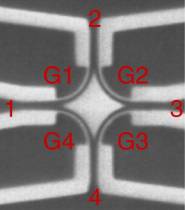
Figure 7. Picture of the PMMA mask in the centre of the device. Bright regions will be etched in the next processing step. The contacts are are numbered consecutively by "1" to "4", the in-plane gates by "G1" to "G4".
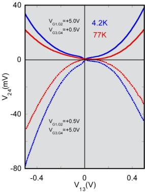
Figure 8. Rectification signal of the device for different gate voltages at 4.2K and 77K.
- A. M. Song et. al., "Nonlinear electron transport in an asymmetric microjunction: A ballistic rectifier.", Phys. Rev. Lett. 80, 3831-3834 (1998).
- R. Fleischmann and T. Geisel, "Meoscopic Rectifiers Based on Ballistic Transport.", Phys. Rev. Lett. 89, 016804 (2002).
- S. de Haan et. al., to be published .
Observing nuclear spin polarization in a quantum dot
Andreas K. Hüttel, J. Weber, and Robert H. Blick
in cooperation with Karl Neumaier and Karl Eberl.
With regard to quantum information processing the details of coupling between electronic and nuclear spins are becoming more and more important for obtaining spin control in a semiconductor chip.
We have observed hysteresis in microwave-induced photocurrent through a quantum dot on a timescale of ~10min: after applying a low magnetic field (B < 0.1T) perpendicular to the 2DES and setting the field back to zero again, the photocurrent trace still displays a distinct shape change, relaxing exponentially. Tuning the system into electron spin resonance using an additional constant magnetic field parallel the 2DES, we see a significant decrease in lifetime of this excitation. A parallel magnetic field alone does not induce any hysteresis effect.
We interpret the hysteresis as the detection of a current-induced nuclear spin polarization and its depolarization. In a spin blockade scenario, the interplay of angular momentum and spin states leads to a controlled and localized dynamical spin polarization transfer into the nuclear lattice. The decay of this polarization is traced by the photocurrent resonance shape.
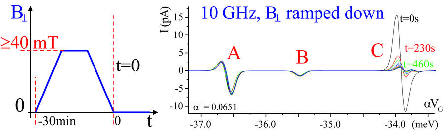
Figure 9. left: sketch of magnetic field ramping up and down; right: subsequent photocurrent traces in the quantum dot; a hysteresis on the order of 10min is observed
- A.K. Hüttel, J. Weber, A.W. Holleitner, D. Weinmann, K. Eberl, and R.H. Blick, "Nuclear spin relaxation probed by a single quantum dot", submitted to Phys.Rev.Lett.
Single-electron effects in highly doped polysilicon nanowires
Armin Tilke, Robert H. Blick, Heribert Lorenz, and Jörg P. Kotthaus
We investigate silicon-based single-electron transistors in thin layers of highly doped recrystallized amorphous silicon. After rapid thermal annealing polysilicon grains have been found with sizes of about 25 nm acting as electron islands. Applying high-resolution electron-beam lithography we have fabricated nanowires with width down to about 10 nm in the polycrystalline silicon films. Single-electron effects in the non-linear source-drain characteristics up to temperatures of about 25 K have been observed.
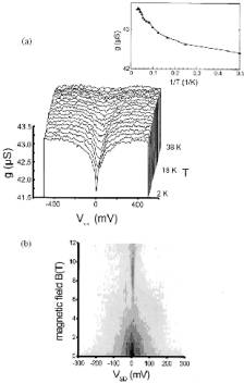
Figure 10. (a) Temperature dependence of the non-linear source-drain characteristics of a 25 nm wide,40 nm high and 500 nm long poly-Si nanowire. The inset shows the temperature dependence of the conductance at zero bias VSD = 0 V. (b) Magnetic field dependence of the conductance at T = 2 K. A second minimum around B ~ 10 T is visible.
- A. Tilke, R. H. Blick, H. Lorenz, and J. P. Kotthaus, Physica E 15, 60-64 (2002)
Electron-phonon interaction in suspended highly doped silicon nanowires
Armin Tilke, Laura Pescini, Heribert Lorenz, and Robert H. Blick
We have realized highly doped suspended silicon nanowires with lateral dimensions down to 20 nm for studying electron transport and dissipation phenomena in these wires. Random dopant fluctuations lead to the formation of multiple tunnel junctions, showing Coulomb blockade phenomena at low drain-source bias. In the finite-bias regime we observe relaxation of hot electrons via phonons. Melting of the wires then occurs at high bias values at an extremely large current density of the order of 1 MA cm-2.
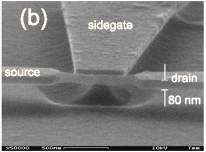
Figure 11. Side view of the smallest suspended silicon nanowire fabricated with a width of 23 nm. The highly doped wire is clearly underetched; the sidegate allows us to tune the carrier density in the wire.
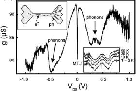
Figure 12. Conductance of the nanowire at high VDS: in the centre the MTJ resonance at 1.5 K is seen. Around ±0.5 V we find structure indicating electron relaxation via phonons at the Brillouin zone edge. The lower right inset shows the insensitivity of the phonon relaxation peaks up to 90 K, which supports the estimation of a wire temperature of about 600 K. The upper left inset schematically illustrates the assumed mechanism of electron thermalization occurring in the clamping points.
- A. Tilke, L. Pescini, A. Erbe, H. Lorenz, and R.H. Blick, Nanotechnol. 13, 491-494 (2002)
Transport properties of freely suspended low-dimensional electron gases
Eva M. Höhberger, J. Kirschbaum, T. Krämer, R. H. Blick in cooperation with Max Bichler and Werner Wegscheider.
Freely suspended nanostructures containing a two-dimensional electron gas can be processed from a GaAs/AlGaAs heterostructure [1]. We have realized free-standing beams in which the 2DEG is constraint by two sets of indentations to form a ballistic cavity (fig.13, inset). In opposition to unsuspended but otherwise identical billiards the magnetoresistance displays a characteristic low-field structure consisting of a pronounced zero-field peak as well as aperiodic resistance oscillations (red and blue in fig. 13, respectively). The additional features can be traced back to coherent back- and forward scattering in a chaotic ballistic cavity, respectively [2]. Applying a negative voltage to a nearby gate electrode the electron system in the free-standing membrane can be depleted to form a quantum dot between the two indentations now acting as tunneling barriers. Single electron tunneling and Coulomb blockade have been observed in the freely suspended quantum dot at a bath temperature of 10 mK [2]. However, single electron tunneling is completely suppressed for small potential bias applied between the reservoirs (fig. 14). This additional blockade effect provides direct evidence of the modified phonon spectrum in the free-standing membrane [3].
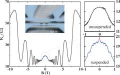
Figure 13. Low-field magnetoresistance of a freely suspended 2DEG.
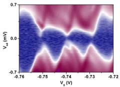
Figure 14. Coulomb blockade in a suspended quantum dot.
- "Magnetotransport in freely suspended two-dimensional electron systems for integrated nanomechanical resonators", E. M. Höhberger, R. H. Blick, F. W. Beil, W. Wegscheider, M. Bichler, and J. P. Kotthaus, Physica E 12, 487 (2002).
- "Integrating suspended quantum dot circuits for applications in nanomechanics", J. Kirschbaum, E. M. Höhberger, R. H. Blick, W. Wegscheider, and M. Bichler, Appl. Phys. Lett. 81, 280 (2002); This paper has been selected for the July 8, 2002 issue of the Virtual Journal of Nanoscale Science & Technology.
- "Electron-phonon interaction in freely suspended quantum dots", E. M. Höhberger, J. Kirschbaum, R. H. Blick, J. P. Kotthaus, and W. Wegscheider, to be published in Physica E.