

E. Nanodevices
Science and technology on the scale of a nanometer -one billionth of a meter- is revolutionary. Nanotechnology refers to the ability to manipulate individual atoms and molecules, making it possible to build machines on the scale of human cells or create materials and structures from the bottom up or from the top down, building in desired properties.
Applications of nanotechnology include:
- Materials with desirable properties such as high strength, chemical sensing or optical switching designed in from the start.
- Information technology by quantum computing and computer chips that store trillions of bits of information on a pin-head device.
- Medical applications with improved drug and gene delivery, biocompatible materials for implants and nanoscale sensors for detection of disease.
The goals of our nanoscale research and engineering are:
- Biosystems at the nanoscale - the relationship among chemical composition, shape and function.
- Nanoscale structures, novel phenomena and quantum control - how to overcome existing limits to miniaturization.
- Device and system architecture - integrating nanoscale devices into measurement and control assemblies.
We investigate realizations of devices fabricated in silicon-on-insulator (SOI)-films, e.g. nanoscale field-emitter devices working at atmospheric pressure. Another goal is to develop electrically driven nanotweezers, which allow a specific manipulation of particles with sizes in the range of some 10 nm.
Other topics of our nanodevice research combine surface acoustic wave technology with biological applications. This can be used for sensing or for the manipulation of small droplets down to the range of femtoliters.
Also, we have developed a planar, microstructured quartz chip for patch clamp measurements to replace the commonly used glass pipettes. Whole cell recordings from different cell types were performed with the microstructured chips.
Our research with nanodevices splits in the following projects:
-
Whole cell patch clamp recordings on a planar glass chip
Niels Fertig, Robert H. Blick, and Jan C. Behrends. -
Acoustically Driven Microfluidic
Christoph Strobl and Achim Wixforth. -
Optical Imaging and Chemical Sensors with Spatial Resolution Based on
Surface Acoustic Wave Devices.
Alexander Müller, Hans-Jörg Kutschera, and Achim Wixforth. -
Nanoscale Lateral Field-Emission Triode Operating at Atmospheric
Pressure
Laura Pescini, Armin Tilke, Robert H. Blick, Heribert Lorenz, and Jörg P. Kotthaus. -
Nanotweezers and Electron Beam Deposition
Christine Meyer, Heribert Lorenz, and Jörg P. Kotthaus.
Whole Cell Patch Clamp Recordings on a Planar Glass Chip
Niels Fertig, Robert H. Blick, and Jan C. Behrends.
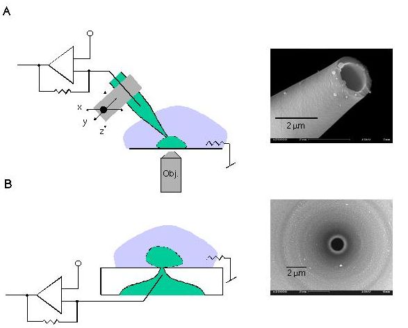
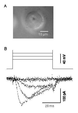
The state of the art technology for the study of ion channels is the patch clamp technique (see fig. 1A). Ion channels mediate electrical current flow, have crucial roles in cellular physiology and are important drug targets. The most popular (whole cell) variant of the technique detects the ensemble current over the entire cell membrane. Patch clamping is still a laborious process, requiring a skilled experimenter to micromanipulate a glass pipette under a microscope to record from one cell at a time. We have developed a planar, microstructured quartz chip for whole cell patch clamp measurements without micromanipulation or visual control (see fig. 1B). A quartz substrate of 200 µm thickness is perforated by wet etching techniques resulting in apertures with diameters of about 1 µm (see fig. 2A). The apertures replace the tip of glass pipettes commonly used for patch clamp recording. Whole cell recordings from different cell types (CHO, N1E-115 neuroblastoma) are performed with microstructured chips studying BK channels and voltage gated Ca2+-channels (see fig. 2B).
Acoustically Driven Microfluidic
Christoph Strobl and Achim Wixforth.
Surface acoustic wave-filters (SAW-filter) can be used to mix and actuate small amounts of liquids. Energy from the surface wave is transferred into the liquid, leading to an effective agitation under certain experimental conditions. We have demonstrated such actuation of liquids for typical volumes between 5µl and 1nl. To observe the internal streaming of the fluid, an optical method using fluorescence dye and a microscope has been developed. At larger RF-power the internal streaming becomes so strong that it is possible to actually move the whole droplet over a smooth surface in the direction of SAW-propagation. To control the direction and trajectory of this movement we modulate the wetting properties of a SiO2-covered LiNbO3-surface defining planar fluidic tracks on the sample surface. Actuation and mixing efficiency were measured as a function of the applied RF-power, RF-signal modulation, RF-frequency and liquid viscosity.
- A. Rathgeber, C. Strobl, H.-J. Kutschera, and A. Wixforth, "Planar microfluidics - liquid handling without walls", to be published.
Optical Imaging and Chemical Sensors with Spatial Resolution Based on Surface Acoustic Wave Devices.
Alexander Müller, Hans-Jörg Kutschera, and Achim
Wixforth,
in cooperation with Thomas Bein,
and Dan C. Driscoll, Micah Hanson, Christoph Kadow,
and Art C. Gossard.
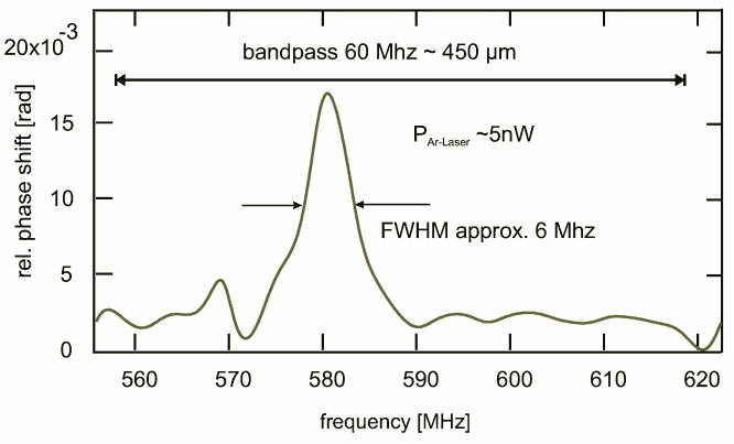
The transmission signal of a surface acoustic wave (SAW) device with so called tapered interdigital transducers (TIDT) is a bandpass. Depending on the applied frequency within such a bandpass, the SAW travels on different, very narrow paths. This is our tool to spatially resolve changes in the transmission properties. The propagation of a SAW is modified with changes in material properties (e.g. changes in conductance due to illumination or additional mass on the delay line). Different materials were examined and TIDT designs were optimized. We found that a very sensitive device to detect weak light signals is a sub micron thick semiconducting GaAs layer on a LiNbO3 128o-cut substrate.
Nanoscale Lateral Field-Emission Triode Operating at Atmospheric Pressure
Laura Pescini, Armin Tilke, Robert H. Blick, Heribert Lorenz, and Jörg P. Kotthaus.
We demonstrated the functioning of a nano-triode, an integrated fully tunable field-emitter, fabricated out of doped SOI material. This lateral nano-triode operates at room temperature and under ambient pressure. The main advantages of this approach are low turn-on voltages and the possibility of direct integration into existing silicon technology. Within this setup it is possible to tune the current collected at the drain electrode by biasing the gate electrodes.
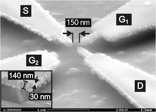
Figure 1. Scanning electron micrograph of the
free-standing silicon nanostructure:
Aerial view of the
device with the contacts marked as source (S), drain (D),
gate 1 (G1), and gate 2 (G2). Inset: Silicon/phosphorus
grains with sizes on the order of 10±30 nm are found on the
edges of the doped substrate, constituting the
field-emission tips.
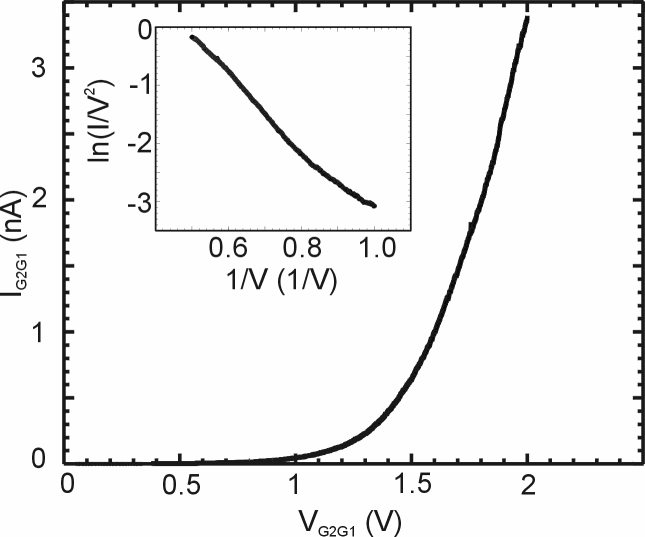
Figure 2. I-V characteristic measured between the contacts G1 and G2 at p = 1 atm and T = 300 K. The bias on the other electrodes is set to zero (VDS = 0) in this case. The inset shows a Fowler-Nordheim plot of ln( I/ V2 ) vs. 1/ V.
- L. Pescini, A. Tilke, R. H. Blick, H. Lorenz, J. P. Kotthaus, W. Eberhardt, and D. Kern, Adv. Mater. 13, 1780-1783 (2001).
Nanotweezers and Electron Beam Deposition
Christine Meyer, Heribert Lorenz, and Jörg P. Kotthaus.
Motivation and aim of this project is to pick up particles with typical sizes in the range of some 10 nm and to release them at a predefined location. Nowadays, the manipulation of nanoparticles is mainly done by atomic force microscopy resulting in a more stochastic displacement. Our goal is to develop electrically driven nanotweezers, which allow a specific manipulation. We demonstrated the fabrication of a tweezers-structure out of SOI material (see figure 3). The tips that are to grip the particles are build out of electron beam deposited material.

Figure 3. Scanning electron micrograph of the silicon nanostructure: Two electron beam deposited tips are grown onto free standing silicon arms.