

C. Static and Dynamic Lateral Superlattices
Surface acoustic waves are modes of elastic energy which can propagate on the surface of different materials. If the substrate is piezoelectric, those waves are accompanied by electric fields which then propagate at the speed of sound. The electric fields of the wave can couple to the mobile carriers within a semiconductor structure and modify its electronic and elastic properties. By measuring the attenuation of the wave and the renormalization of the sound velocity we can, for instance, extract information on the dynamic conductivity of the electron system. We also investigate the possibility to use a SAW for a dynamical lateral potential modulation and we study the influence of a SAW onto the optical properties of an electron system. Static superlattices can be used as another method to influence the optical properties of a semiconductor sample. Also, quantum dots are employed to modify the emission properties of the sample. Our experiments presently cover the frequency range between 100 MHz and 6 GHz, corresponding to surface acoustic wavelengths between 30 and 500 nm, respectively.
The SAW - related research in 2001 was structured in the following topics:
-
Storage of Electrons and Holes in Static
Lateral Superlattices
Jan Krauß, Alexander V. Kalameitsev, Alexander O. Govorov, Achim Wixforth, and Jörg P. Kotthaus. -
Imaging of the Interaction of Surface Acoustic Waves with Excitons
Christoph Bödefeld, Hans-Jörg Kutschera, and Achim Wixforth. -
Acoustic Pumping of Semiconductor Quantum Dots
Christoph Bödefeld and Achim Wixforth. -
Nonlinear Acoustoelectric and Acoustooptic Effects
Hans-Jörg Kutschera, Achim Wixforth, Alexander V. Kalameitsev, and Alexander O. Govorov.
Storage of Electrons and Holes in Static Lateral Superlattices
Jan Krauß, Alexander V. Kalameitsev, Alexander O. Govorov,
Achim Wixforth, and Jörg P. Kotthaus,
in cooperation with Dan C. Driscoll, Micah Hanson, Christoph Kadow,
Art C. Gossard,
and Dieter Schuh, Max Bichler, Werner Wegscheider.
Strong lateral potential modulation in semiconductor heterostructures can be achieved by voltages applied to interdigitated metal electrodes on top of the structure. This modulation can be tuned and even be switched "on" and "off" according to the particular voltages.
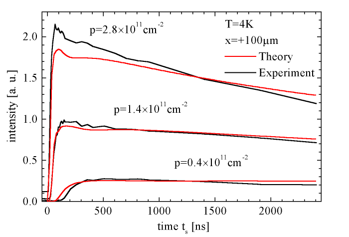
In particular, the modulation can be used to spatially separate photogenerated electron-hole-pairs, thus increasing recombination lifetime by orders of magnitudes. Removing the voltage triggers radiative recombination which can be utilized as "photonic memory" [1]. We used this effect to visualize Maxwell relaxation of a two-dimensional hole plasma using a special snapshot-technique which allows us to record "Movies" of the charge evolution:
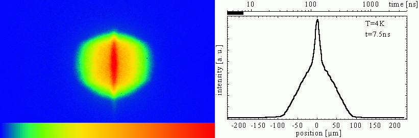
Figure 1. The luminescence image, which corresponds to the distribution of holes is shown in the left part. The width of the image is about 500 µm. The color coding of the intensity scale is given below, ranging from blue (dark) to red (bright). Due to the sample structure, motion is only possible horizontally. In the right picture, a horizontal cross-section of the image is shown together with the actual delay time for each frame (see the animated gif ).
Maxwell relaxation in two dimensions has the particular feature of "charge spreading", i. e. the broadening of the distribution due to electrostatic repulsion. We were able to study this effect in a strongly nonlinear regime where the initial dynamics slow down considerably due to dilution of the carrier distribution. The image shows the temporal evolution at different initial densities. The agreement with numerical simulations is very accurate [2].
- S. Zimmermann, A. Wixforth, J. P. Kotthaus, W. Wegscheider, and M. Bichler, "A Semiconductor Based Photonic Memory Cell", Science 283, 1292-1295 (1999).
- J. Krauß, A. Wixforth, A. V. Kalameitsev, A. O. Govorov, W. Wegscheider, and J. P. Kotthaus, "Nonlinear Charge Spreading Visualized in Voltage-Controlled Lateral Superlattices", Phys. Rev. Lett. 88, 036803 (2002).
Imaging of the Interaction of Surface Acoustic Waves with Excitons
Christoph Bödefeld, Hans-Jörg Kutschera, and Achim
Wixforth,
in cooperation with Dan C. Driscoll, Micah Hanson, Christoph Kadow,
Art C. Gossard.
With an intensified and gated CCD, we can now record images of a semiconductor heterostructure at 4 K with a time and spatial resolution of minimal 300 ps and 1µm respectively. As an example we record the change in photoluminescence (PL) intensity with an surface acoustic wave (SAW) applied (see figure). As one can easily see, the PL is modified in two ways: It is decreased in the peak and increased right in front of the main pulse. Whereas the first effect is due to the so called quenching of the PL [1], the second is based on an increased emission rate of surface states [2]. With this imaging technique it is now possible to record the temporal evolution of the SAW pulse (see the movie here).
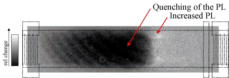
Figure 2. Image of a surface acoustic wave propagating on a semiconductor heterostructure, 600 ns after emission from the left interdigital transducer. The photoluminescence induced from a laser is strongly modulated by the SAW.
- C. Rocke et al., Phys. Rev. Lett. 78, 4099 (1997).
- D. Janes et al., J. Appl. Phys. 67, 6315 (1990).
Acoustic Pumping of Semiconductor Quantum Dots
Christoph Bödefeld and Achim Wixforth,
in cooperation with Juha Toivonen, Markku Sopanen, and Harri
Lipsanen.
We investigate the acoustic pumping of self-organised stress-induced quantum dots. We excite excitons with above bandgap radiation of a laser diode. In the strong electric potential of a SAW these excitons are ionised and trapped. The trapped carriers move with the wave in its lateral potential until a quantum dot is passed. With a high probability the carriers are caught by the deep potential of the dot. If two complementary carriers are caught by the same quantum dot, recombination can take place and a photon is emitted. Due to the strict periodic nature of this pumping process [1], the emitted light itself is modulated with the frequency of the SAW. For a small area on the sample (approx. 1000 dots) this is shown in the figure below.
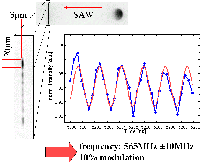
Figure 3. Time dependence of the quantum dot photoluminescence in a small part of the sample (20µm x 3µm) due to the regular pumping mechanism. The frequency of the modulation matches the frequency of the wave.
- C. Wiele, F. Haake, C. Rocke, and A. Wixforth, "Photon trains and lasing: The periodically pumped quantum dot", Phys. Rev. A 58, R2680 (1998).
- C. Bödefeld, A. Wixforth, J. Toivonen, M. Sopanen and H. Lipsanen, "Pumping of Quantum Dots with Surface Acoustic Waves", phys. stat. sol. (b) 224, 703 (2001).
Nonlinear Acoustoelectric and Acoustooptic Effects
Hans-Jörg Kutschera, Achim Wixforth, Alexander V. Kalameitsev,
and Alexander O. Govorov,
in cooperation with Dan C. Driscoll, Micah Hanson, Christoph Kadow,
Art C. Gossard.
We study experimentally the interaction of intense surface acoustic waves with an electron and an electron-hole plasma of a quantum well. The experiments performed on hybrid semiconductor-piezocrystal structures exhibit strong nonlinear acoustoelectric and acoustooptic effects due to the formation of moving electron and electron-hole wires, respectively. It was shown theoretically that the nonlinear interaction of a SAW with a photo-generated electron-hole plasma qualitatively differs from the case of an unipolar electron system [1]. For low temperatures in the regime when the intense SAW forms moving quantum wires or quantum dots we expect a novel quantum acoustic phenomenon: self-induced acoustic transparency [2].
- A. V. Kalameitsev, A. O.Govorov, H.-J. Kutschera,
A. Wixforth, JETP Letter 72, 190 (2000);
A. O. Govorov, A. V. Kalameitsev, M. Rotter, A. Wixforth, J. P. Kotthaus, K.-H. Hoffmann, N. Botkin, Phys. Rev. B 62, 2659 (2000). - A. O. Govorov, A. V. Kalameitsev, V. M. Kovalev, H.-J. Kutschera, and A. Wixforth, Phys. Rev. Lett. 87, 226803 (2001).