

A. Electronic Properties of Nanostructures
Non-diffusive electronic transport phenomena that display characteristics of semiconductor nanostructures are investigated at low temperatures in a variety of devices, mostly fabricated out of layered semiconductor structures employing the high resolution electron beam lithography in our clean room. Following a proposal by R. Fleischmann we study further the transport mechanisms that cause non-linear ballistic rectification in asymmetric cross-junctions carved out of a two-dimensional electron gas (2DEG) on GaAs. In quantum dots electrostatically induced in a 2DEG on GaAs we investigate at lowest temperatures (<1K) phase coherent transport by embedding two quantum dots in an Aharonov-Bohm ring. In similar quantum dots with suitably chosen spin configuration in the electronic ground state we observe spin blockade of single electron transport. Out of layered silicon-on-insulator systems we are able to fabricate ultra small quantum dots and quantum wires that exhibit single electron transport phenomena at comparably high temperatures. Conduction through quantum wires we study also on bridge-like suspended carbon nanotubes up to infrared frequencies. A newly developed low temperature scanning probe instrument enables us to measure extremely small electrostatic forces and to image potential landscapes and individual charges close to surfaces. Further details can be found via the links below.
-
Ballistic Rectifier
Stefan de Haan, Axel Lorke, and Jörg P. Kotthaus. -
Aharonov-Bohm Interferometry with Quantum Dots
Alexander W. Holleitner, Robert H. Blick, and Jörg P. Kotthaus. -
Ground State Spin Blockade in a Multi-Electron Quantum
Dot
Andreas K. Hüttel, Robert H. Blick, and Jörg P. Kotthaus. -
Fabrication and Integration Possibilities of Ultrasmall
Quantum Dots in Silicon-on-Insulator Material
Armin Tilke, Robert H. Blick, and Heribert Lorenz. -
Single-Electron Tunneling in Highly Doped Silicon
Nanowires in a Dual-Gate Configuration
Armin Tilke, Robert H. Blick, Heribert Lorenz, and Jörg P. Kotthaus. -
Electrical and Mechanical Properties of Carbon Nanotubes
Christian Schäflein, Udo Beierlein, and Jörg P. Kotthaus. -
Low Temperature Scanning Probe Microscopy of Surface and
Sub-Surface Charges
Markus Vogel, Bernhard Stein, Hakan Pettersson, and Khaled Karraï.
Ballistic Rectifier
Stefan de Haan, Axel Lorke, and Jörg P. Kotthaus,
in cooperation with Max Bichler and Werner Wegscheider.
It has been shown earlier in our group that symmetry-breaking strongly influences the transport properties of mesoscopic semiconductor structures. The rectification effect observed in a device consisting of a cross junction with an embedded triangular antidot, can be explained in a simple ballistic picture [1].
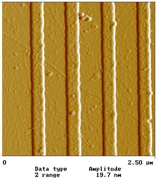
In order to obtain a better understanding of the mechanism responsible for rectification, we investigated a Ballistic Rectifier with a design following a proposal of R. Fleischmann. As seen in the AFM picture (see fig. 1), the central region of the device is formed by four electronic channels of widths such that the symmetry is broken with regard to the source-drain axis.
If the voltage applied to a gate electrode that is covering the entire structure is sufficiently low, we observe clear rectification: The voltage induced between the U and the L channel does not change sign, when the input current is reversed (see fig. 2). Compared to previous experiments, the value of the output voltage is increased by a factor of three, indicating that rectification in the device shown here is more effective.
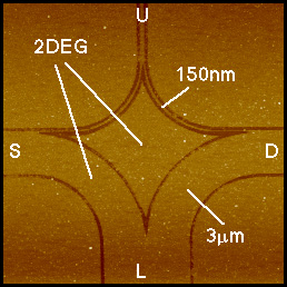
Figure 1. AFM picture of the central part of the device. Dark regions are etched. The contacts are labeled by S ("source"), D ("drain"), U ("upper") and L ("lower").
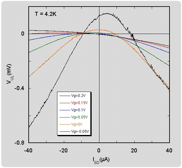
Figure 2. I-V curves VUL vs ISD of the device for different gate voltages.
- A. M. Song et. al., "Nonlinear electron transport in an asymmetric microjunction: A ballistic rectifier.", Phys. Rev. Lett. 80, 3831-3834 (1998).
Aharonov-Bohm Interferometry with Quantum Dots
Alexander W. Holleitner, Robert H. Blick, and Jörg
P. Kotthaus,
in cooperation with Karl Eberl.
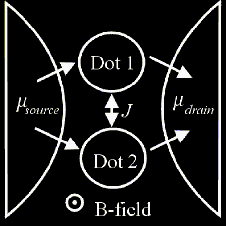
Integrating quantum dots into Aharonov-Bohm (AB) interferometers [1] provides experimental access to the quantum mechanical phase of electrons tunneling through binding states of covalently bound quantum dots [2,3]. As it was proposed theoretically [4], this even allows testing of non-locality and entanglement of singlet- and triplet-states within the double dot system. Below our experimental set-up is sketched: an incoming electron wave function in the source contact splits into two partial waves tunneling via two different quantum dots before recombining in the drain lead. An applied magnetic field changes the relative phase of the partial waves and hereby the overall conductance. In order to realize this AB-interferometer we define parallel few-electron quantum dots within a two-dimensional electron gas of an AlGaAs/GaAs heterostructure, by applying negative voltages to Schottky-gates which are evaporated onto the surface. For decoupled quantum dots with less than 15 electrons each, we find oscillatory AB-conductance for each flux quanta h/e within the device. Dephasing time and length of the mesoscopic system are extracted [5] and furthermore, we demonstrate that charge transport through both quantum dots is partly phase coherent [6]. In addition, we measure the magnetic field dependence of the coherent coupling J of the two quantum dots. Our findings substantiate this coupling J being a many body wave function overlap of dot electrons [6].
- Y. Aharonov and D. Bohm, Phys. Rev. 115, 485 (1959).
- A. Yacoby, M. Heiblum, D. Mahalu and Hadas Shtrikman, Phys. Rev. Lett. 74, 4047 (1995).
- R. H. Blick, D. Pfannkuche, R. J. Haug, K. V. Klitzing, and K. Eberl, Phys. Rev. Lett. 80, 4032 (1998).
- D. Loss and E. V. Sukhorukov, Phys. Rev. Lett 84, 1035 (2000).
- A. W. Holleitner, H. Qin, R. H. Blick, K. Eberl, and J. P. Kotthaus, accepted in Physica E (2001).
- A. W. Holleitner, C. R. Decker, H. Qin, K. Eberl and R. H. Blick, Phys. Rev. Lett. 87, 256802 (2001).
Ground State Spin Blockade in a Multi-Electron Quantum Dot
Andreas K. Hüttel, Robert H. Blick, and Jörg
P. Kotthaus,
in cooperation with Karl Neumaier,
and Dietmar Weinmann,
and Karl Eberl.
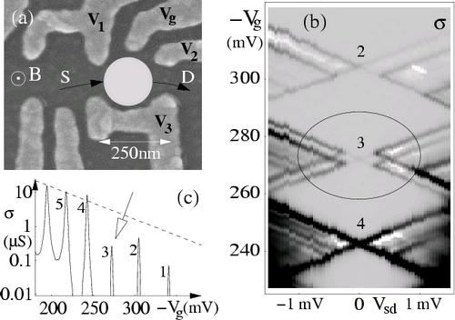
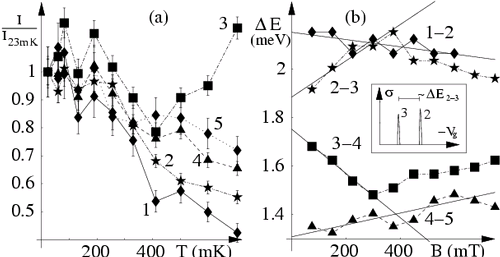
Particularly with respect to spintronics and quantum information processing, the electronic spin degree of freedom in quantum dots has recently attracted considerable interest. In a quantum dot electrostatically defined in the 2DES of an AlGaAs/GaAs heterostructure, we find strong evidence for ground state spin blockade, i.e. suppression of SET current at low bias by spin selection rules (see Fig. 1, peak 3). We confirm many properties predicted for such a system having high spin difference between N-electron and N+1-electron ground state, including temperature, bias, and B-dependence of the transport spectrum. For example, Fig. 2(b) gives the B-dependence of the electron addition energy for subsequent electron numbers, the large slopes at low B indicate a change in dot ground state spin of 5/2 when adding an electron at SET peak 3. Estimates for the lifetime of the spin state and for the spin quantum numbers present are given.
- A. K. Hüttel, H. Qin, A. W. Holleitner, R. H. Blick, K. Neumaier, D. Weinmann, K. Eberl, and J. P. Kotthaus, "Spin blockade in many-electron ground state resonances of a quantum dot", subm. to Phys. Rev. Lett., cond-mat/0109104.
Fabrication and Integration Possibilities of Ultrasmall Quantum Dots in Silicon-on-Insulator Material
Armin Tilke, Robert H. Blick, and Heribert Lorenz.
Single-electron transistors utilizing Coulomb blockade effects are promising candidates for future silicon based nanoelectronics. We present the fabrication of such transistors and measurements that reveal Coulomb blockade behavior. Various silicon quantum dots are investigated up to room temperature. We employ a dual gate configuration with which we are able to control our devices by both a metallic top gate as well as by an in-plane gate. This design principle enhances the integration density.
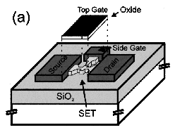
Figure 3. Sketch of a dual gate quantum dot structure. Highly doped source and drain contacts are connected by the laterally structured inversion layer in the SOI film. An in-plane side gate is also defined in the inversion layer and contacted by a strongly doped region.
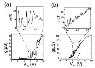
Figure 4. Coulomb blockade oscillations in two inversion quantum dots at a temperature of 2 K. While the oscillations in (a) (dot 1) display no periodicity with VTG, the peaks in trace (b) (dot 2) are almost perfectly equidistant.
- A. Tilke, R. H. Blick, and H. Lorenz,
J. Appl. Phys. 90, 942-946 (2001)
[2] A. Tilke, F. C. Simmel, R. H. Blick, H. Lorenz, and J. P. Kotthaus, Progress in Quantum Electronics 25, 97-138 (2001)
Single-Electron Tunneling in Highly Doped Silicon Nanowires in a Dual-Gate Configuration
Armin Tilke, Robert H. Blick, Heribert Lorenz, and Jörg P. Kotthaus.
Lateral patterning of highly doped silicon-on-insulator films allows us to observe conductance oscillations due to single-electron charging effects. In our devices, silicon nanostructures are embedded into a metal-oxide-silicon configuration. The single-electron effects can be tuned both by an in-plane sidegate, as well as by a metallic topgate, a technology which is compatible with large-scale integration of single-electron devices with dimensions down to 10 nm. We compare the influence of different gating electrodes, important for ultralarge scale integration, on the electron islands.
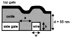
Figure 5. Sketch of the device: The in-plane sidegate is located at a distance a = 95 nm from the silicon nanowire with a width w = 10 nm and a length of l = 500 nm. The silicon film thickness is estimated to be about h = 25 nm. Both structures are embedded into SiO 2, acting as gate oxide with a thick-ness of d = 55 nm. On top, a NiCr/Au gate is located, controlling the electric potential in both the nanowire and the sidegate.
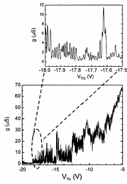
Figure 6. Single-electron effects in a highly doped, 10 nm wide silicon wire at T = 2 K as a function of the topgate voltage VTG. Although almost periodic conductance oscillations can be found, both the peak amplitudes as well as the exact peak positions differ between subsequent gate sweeps.
- A. Tilke, R. H. Blick, H. Lorenz, and J. P. Kotthaus,
J. Appl. Phys. 89, 8159-8162 (2001).
[2] A. Tilke, F. C. Simmel, R. H. Blick, H. Lorenz, and J. P. Kotthaus, Progress in Quantum Electronics 25, 97-138 (2001).
Electrical and Mechanical Properties of Carbon Nanotubes
Christian Schäflein, Udo Beierlein,
and Jörg P. Kotthaus,
in cooperation with the biophysics group of Hermann Gaub.
Carbon nanotubes are two-dimensional graphene sheets rolled into nanometer diameter cylinders that can either be 1D metals or semiconductors, depending on how the sheet is rolled up. During the last years a lot of work has been carried out concerning single wall and multi wall carbon nanotubes (SWNT, MWNT). However, many interesting issues remain open. We study suspended carbon nanotubes at low temperatures. SWNTs and MWNTs were connected to lithographically defined gold leads (see figure). The underlying substrate was removed by a wet etch process in order to obtain freely suspended nanotubes. We then performed dc-transport and far-infrared photoconductivity measurements on single suspended SWNTs and MWNTs.
Low-Temperature Scanning Probe Microscopy of Surface and Subsurface Charges
Markus Vogel, Bernhard Stein, Hakan Pettersson, and Khaled Karraï.
The operation of a cryogenic scanning force microscope is demonstrated with a sensitivity of about 50 fN / Hz1/2 at 5 kHz modulation. This microscope is used as an electrometer in noncontact mode in order to map the local electrostatic forces and capacitance of several nanostructures at 4.2 K. Capacitance imaging of nanostructured surfaces with subatto-Farad resolution is demonstrated.
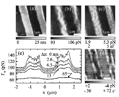
Figure 7. Scanning force microscopy at cryogenic temperatures. a) Topography of the Al0 O3 stripes (bright) on a gold back contact (dark). (b) and (c) Corresponding harmonic and second harmonic forces. The resulting local charge distribution is shown in (d). The line scans of first harmonic forces are shown in (e) for decreasing tip-to-gold-contact . The noise-like features in (e) over the Al 2 O 3 stripes are fully reproducible and represent single electronic charges.
- M. Vogel, B. Stein, H. Pettersson, and K. Karraï, "Low Temperature Scanning Probe Microscopy of Surface and Sub-Surface Charges", Appl. Phys. Lett. 78, 2592-2594 (2001).