Nanophotonics Group
print


Inhaltsbereich

Research interests

Spectroscopy of layered semiconductors and heterostructures

spectroscopy
The primary tool to study light-matter interactions of excitons in layered semiconductors and heterostructures is optical spectroscopy, including complementary methods of absorption, continuous-wave or time-resolved photoluminescence and magneto-luminescence at cryogenic temperatures down to a few tens of mK.
Specific sample realizations include transition metal dichalcogenides (TMDs) with varying dielectric environments and charge carrier control as provided by field-effect van der Waals heterostructures. We use both commercial materials and TMD monolayers, bilayers and heterobilayers from in-house chemical vapor deposition (CVD) synthesis.
In our laboratories, we operate modular fiber-based home-built confocal microscopes optimized for cryogenic operation in liquid-helium and closed-cycle cryostats or a dilution refrigerator with and without magnetic fields. Various lasers and light-sources, high-end spectrometers, time-resolved measurement techniques, single-photon detectors, and full control of the polarization of light support our studies of different types of excitons in monolayers and van der Waals heterostructures [1-4].
  1. Moiré excitons in MoSe2-WSe2 heterobilayers and heterotrilayers
    M. Förg, A. S. Baimuratov, S. Yu. Kruchinin, I. A. Vovk, J. Scherzer, J. Förste, V. Funk, K. Watanabe, T. Taniguchi, A. Högele
    Nat. Commun. 12, 1656 (2021) — PDF
  2. Exciton g-factors in monolayer and bilayer WSe2 from experiment and theory
    J. Förste, N. V. Tepliakov, S. Yu. Kruchinin, J. Lindlau, V. Funk, M. Förg, K. Watanabe, T. Taniguchi, A. S. Baimuratov, A. Högele
    Nat. Commun. 11, 4539 (2020) — PDF
  3. Signatures of defect-localized charged excitons in the photoluminescence of monolayer molybdenum disulfide
    A. Neumann, J. Lindlau, M. Nutz, A. D. Mohite, H. Yamaguchi, A. Högele
    Phys. Rev. Materials 2, 124003 (2018) — PDF
  4. The role of momentum-dark excitons in the elementary optical response of bilayer WSe2
    J. Lindlau, M. Selig, A. Neumann, L. Colombier, J. Förste, V. Funk, M. Förg, J. Kim, G. Berghäuser, T. Taniguchi, K. Watanabe, F. Wang, E. Malic, A. Högele
    Nat. Commun. 9, 2586 (2018) — PDF

Quantum optoelectronics with van der Waals heterostructures

Quantum optoelectronics with van der Waals heterostructures
The large exciton binding energy and oscillator strength make transition metal dichalcogenides (TMDs) attractive candidates for cavity quantum electrodynamics (QED) experiments. Our current research projects focus on engineering light-matter interactions with a tunable fiber-based Fabry-Pérot micro-cavity to study Purcell-enhancement in the weak-coupling regime [2] and observe exciton-polaritons in the strong-coupling regime [1, 3]. One of our on-going research project aims at creating exciton-polariton lattices by structuring the photonic or the excitonic two-dimensional landscape. More advanced experiments will eventually aim at controlling exciton-polariton currents in novel quantum optoelectonic devices.
  1. Open-cavity in closed-cycle cryostat as a quantum optics platform
    S. Vadia, J. Scherzer, H. Thierschmann, C. Schäfermeier, C. Dal Savio, T. Taniguchi, K. Watanabe, D. Hunger, K. Karrai, A. Högele
    arXiv:2103.05619 [quant-ph] (2021) — PDF
  2. Cavity-control of interlayer excitons in van der Waals heterostructures
    M. Förg, L. Colombier, R. K. Patel, J. Lindlau, A. D. Mohite, H. Yamaguchi, M. M. Glazov, D. Hunger, A. Högele
    Nat. Commun. 10, 3697 (2019) — PDF
  3. Polariton hyperspectral imaging of two-dimensional semiconductor crystals
    C. Gebhardt, M. Förg, H. Yamaguchi, I. Bilgin, A. D. Mohite, C. Gies, M. Florian, M. Hartmann, T. W. Hänsch, A. Högele, D. Hunger
    Sci. Rep. 9, 13756 (2019) — PDF

Theory of optical excitation in layered semiconductors

Theory of optical excitation in layered semiconductors
In conjunction with our experimental expertise we develop theory of fundamental optical properties of layered semiconductors and heterostructures [1-3]. This instructive interplay is highlighted by our most recent publications on magneto-optics of excitons in monolayer and bilayer transition metal dichalcogenides [3] and heterobilayer and heterotrilayer systems [1]. In both studies, we used high magnetic fields of up to 9 T to characterize various exciton species by their respective magneto-induced spectral splitting known as the valley Zeeman splitting. This splitting, proportional to the exciton g-factor, can serve as an unambiguous signature of diverse spin and valley configurations of excitons. Without theory, however, it is merely a phenomenological number. The key aspect of our work therefore was the development of theoretical methods to predict from first principles the exciton g-factors for all possible spin-valley configurations in different realizations of layered systems.
  1. Moiré excitons in MoSe2-WSe2 heterobilayers and heterotrilayers
    M. Förg, A. S. Baimuratov, S. Yu. Kruchinin, I. A. Vovk, J. Scherzer, J. Förste, V. Funk, K. Watanabe, T. Taniguchi, A. Högele
    Nat. Commun. 12, 1656 (2021) — PDF
  2. Valley-selective energy transfer between quantum dots in atomically thin semiconductors
    A. S. Baimuratov, A. Högele
    Sci. Rep. 10, 16971 (2020) — PDF
  3. Exciton g-factors in monolayer and bilayer WSe2 from experiment and theory
    J. Förste, N. V. Tepliakov, S. Yu. Kruchinin, J. Lindlau, V. Funk, M. Förg, K. Watanabe, T. Taniguchi, A. S. Baimuratov, A. Högele
    Nat. Commun. 11, 4539 (2020) — PDF

Synthesis of two-dimensional semiconductors and heterostructures

Synthesis of two-dimensional semiconductors and heterostructures
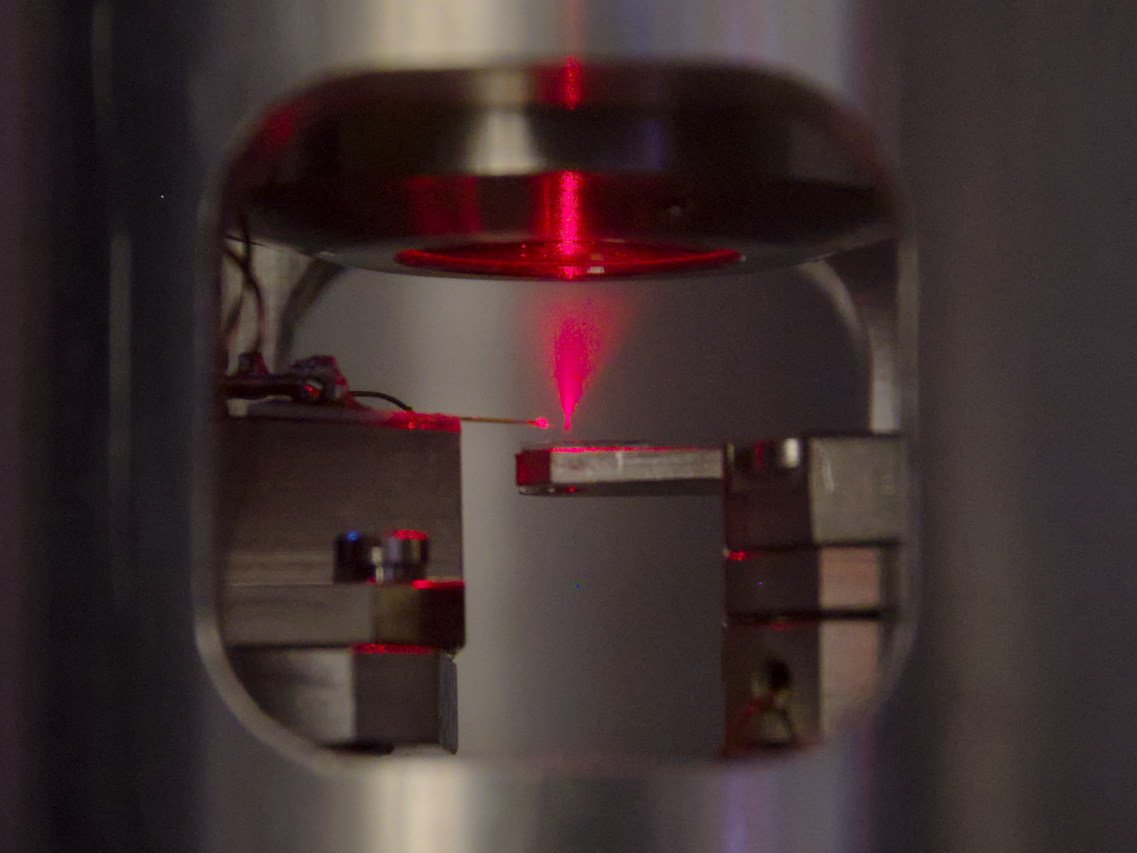
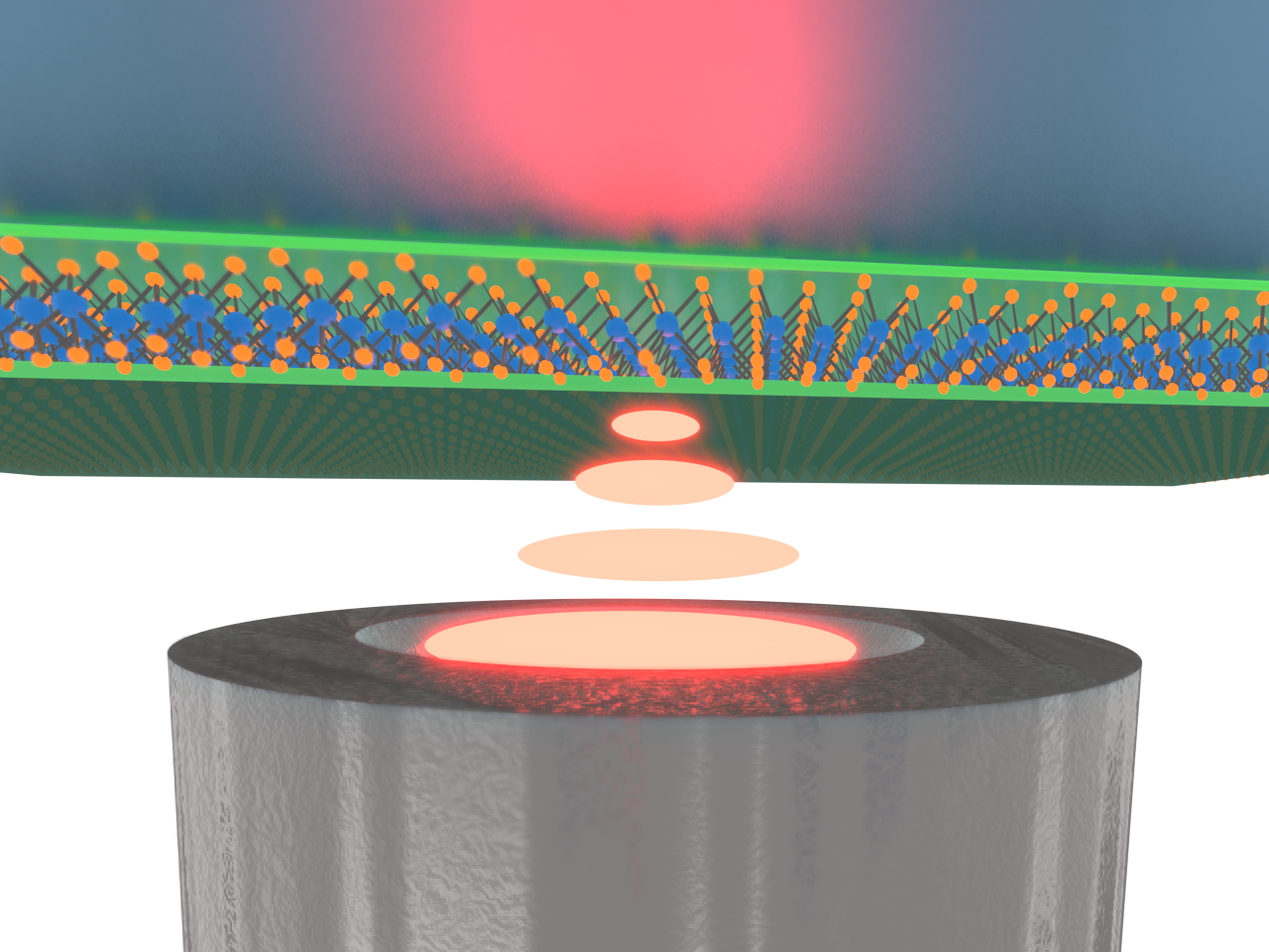
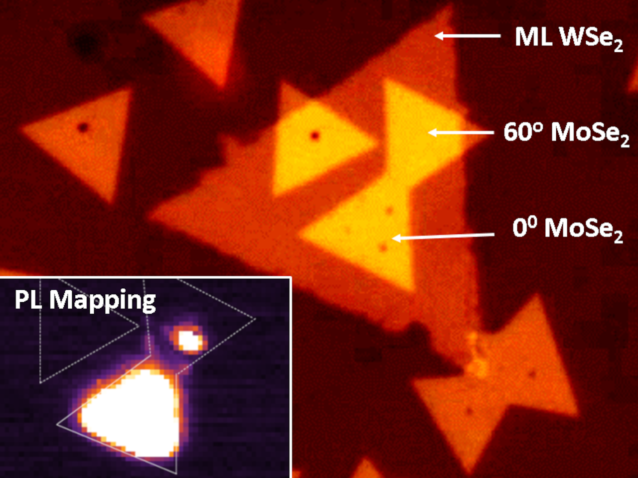
Two–dimensional transition metal dichalcogenides (e.g MoS2, MoSe2, WS2, WSe2) are easy to obtain by mechanical exfoliation, however, only with limited lateral dimensions. In contrast to mechanically exfoliated samples, optimized chemical vapor deposition (CVD) synthesis not only yields laterally extended single-crystal monolayers or bilayers, it also allows to control the material composition (such as MoxW1-xSe2) or realize lateral and vertical heterostructures (such as MoSe2-WSe2) with atomically sharp interfaces. We continuously work on optimizing synthesis parameters towards material quality, reproducibility and yield, to establish deterministic growth methods for large-area monolayers and heterostructures as elementary semiconductor building blocks of van der Waals devices with increasing complexity and functionality for quantum optics applications.

Carbon nanotubes

Carbon nanotubes
Optical emission from semiconducting single-wall carbon nanotubes covers a broad spectral window from the visible to the infrared. When cooled down to low temperatures, single carbon nanotubes show photon emission statistics that are characteristic of quantum emitters: they emit merely one photon at a time. This feature – ensured by exciton localization as a generic feature of cryogenic nanotubes – can be exploited in single-photon emission devices for quantum communication in the telecom band. Our collaboration partners for carbon nanotube materials are J.A. Fagan, National Institute of Standards and Technology (NIST), USA and Y. Wang, University of Maryland University, USA.
  1. Environmental Electrometry with Luminescent Carbon Nanotubes
    J. C. Noé, M. Nutz, J. Reschauer, N. Morell, I. Tsioutsios, A Reserbat-Plantey, K. Watanabe, T. Taniguchi, A. Bachtold, A. Högele
    Nano Lett. 18, 4136–4140 (2018) — PDF
  2. Dipolar and charged localized excitons in carbon nanotubes
    J. T. Glückert, L. Adamska, W. Schinner, M. S. Hofmann, S. K. Doorn, S. Tretiak, A. Högele
    Phys. Rev. B 98, 195413 (2018) — PDF
  3. Cavity-enhanced Raman microscopy of individual carbon nanotubes
    T. Hümmer, J. Noé, M. S. Hofmann, T. W. Hänsch, A. Högele, D. Hunger
    Nat. Commun. 7, 12155 (2016)
  4. Ubiquity of exciton localization in cryogenic carbon nanotubes
    M. S. Hofmann, J. Noé, A. Kneer, J. J. Crochet, A. Högele
    Nano Lett. 16, 2958–2962 (2016)
  5. Bright, long-lived and coherent excitons in carbon nanotube quantum dots
    M. S. Hofmann, J. T. Glückert, J. Noé, C. Bourjau, R. Dehmel, A. Högele
    Nature Nanotech. 8, 502-505 (2013)