Electronic coupling effects in self-
assembled InAs quantum dots
R.J. Luyken, A. Lorke, M. Haslinger, B.T. Miller, M. Fricke, and J.P.
Kotthaus
Sektion Physik, LMU München, Geschwister-Scholl Platz 1, 80539
München, Germany
G. Medeiros-Ribeiro and P.M. Petroff
Materials Department / QUEST, University of California, Santa Barbara, CA
93106, USA
Electronic coupling effects in self-assembled InAs quantum dots are
investigated using capacitance and far-infrared (FIR) spectroscopy. Coupling
between different dot-layers is studied using capacitance spectroscopy on
samples with double-layers of vertically aligned quantum dots. A strong
electrostatic dot-dot interaction reveals itself in distinct shifts of the
many particle ground state energies. The fact that the line widths of the FIR
resonances are typically a factor of three narrower than expected from the
inhomogenous broadening due to size fluctuations of the dots is attributed to
lateral coupling between the dots within the plane of the dot ensemble.
Keywords: GaAs/InAs; self assembled quantum dot, coupling
Correspondence address :
Axel Lorke
Sektion Physik, LMU München, Geschwister-Scholl Platz 1, 80539
München, Germany Fax +49 89 2180 31 82; email:
axel.lorke@physik.uni-muenchen.de
Recently, self-assembled quantum dots have gained particular interest as they
provide for well defined, nm-size quantum dots with sizes in the 10 nm range
[1,2,3]. For possible device applications it is of fundamental interest to know
the effects of dot-dot interactions as they could on the one hand limit the
integration density, but on the other hand might offer the possibility to
implement new computational concepts [4].
Here we study the effects of the static and dynamic Coulomb interaction in
large-scale dot ensembles. The samples are grown by molecular beam epitaxy
using the Stranski-Krastanov growth procedure to create self-assembled InAs
dots [5]. The dots are embedded into a suitably designed MISFET
(metal-insulator-semiconductor-field-effect-transitor) type GaAs/ AlGaAs
heterostructure as described in Refs. [2,3]. Fig. 1 shows the essential layer
sequence and a sketch of the conduction band edge for the investigated
double-layer samples. The dots in the second layer are aligned along the
growth direction to the dots of the first layer as the strain field of the
first dot acts as a nucleus for the growth of the second one [6]. Except for
the second dot layer, the single layer samples are identical. From atomic force
micrographs of similar grown samples we estimate the InAs dots to be
approximately 20 nm in diameter and 6 nm in height [5].
The samples are provided with Ohmic contacts and a semi-transparent gate. They
are then mounted in a liquid He cryostat equipped with a superconducting
solenoid, capable of producing fields of up to B=15 T perpendicular to the
plane of the dots. The FIR transmission of the sample is recorded using a
rapid-scan-Fourier-transform spectrometer, the capacitance-voltage (CV) spectra
are measured by standard lock-in technique.
Vertical coupling is investigated on double-layer samples with vertically
aligned quantum dots with separation of 10 and 20 nm. In order to investigate
possible quantum mechanical coupling effects we first calculate the
single-particle energy splitting between two levels of different dots using a
simple model of a double quantum well. With the given values for our system we
obtain even for the 10 nm sample an energy splitting of only 100 ueV. This is
far beyond the limit of resolution due to inhomogenous size broadening of our
dot ensembles. Therefore, the dominant type of interaction observed in the CV
spectra of vertically aligned double quantum dots is the Coulomb interaction
between the dots of different layers.
Fig. 2 (a) shows a CV trace of the sample A ( 20 nm dot-dot distance). For
comparison, CV traces from a single-layer sample and a sample with only two
wetting layers are also shown (b),(c). For negative gate voltages the spectra
of the double -dot sample is the same than for the single layer one. As
described in detail for single-layer samples in Ref. [3] the double peak at
Vg
 -1V corresponds to the filling of the lowest (s-) state of the quantum dots.
The s-state is doubly spin degenerate and the difference in the gate voltage
between loading of the first and the second electron is a direct consequence of
the Coulomb blockade caused by electron-electron interaction within one dot. In
our oblate, nearly circular dots the second shell is fourfold degenerate and,
because of Coulomb repulsion, we expect four peaks at higher gate voltage, when
the p-state is gradually filling. In contrast to earlier investigations we
could resolve for the first time loading of distinct p-states within such a
large ensemble of dots (approx. 108), which is depicted in the inset
of Fig. 2. We attribute this to improved growth conditions which result in a
further narrowed dot size distribution.
-1V corresponds to the filling of the lowest (s-) state of the quantum dots.
The s-state is doubly spin degenerate and the difference in the gate voltage
between loading of the first and the second electron is a direct consequence of
the Coulomb blockade caused by electron-electron interaction within one dot. In
our oblate, nearly circular dots the second shell is fourfold degenerate and,
because of Coulomb repulsion, we expect four peaks at higher gate voltage, when
the p-state is gradually filling. In contrast to earlier investigations we
could resolve for the first time loading of distinct p-states within such a
large ensemble of dots (approx. 108), which is depicted in the inset
of Fig. 2. We attribute this to improved growth conditions which result in a
further narrowed dot size distribution.
After filling of the p-shell, the double-dot system behaves differently than
the single-dot system: In addition to the charging of the wetting layer and the
2D electron gas at the GaAs/ GaAlAs interface we observe three additional peaks
in the 20 nm double dot sample (labelled sdot2, pdot2, x
in Figs. 2,3), which show the charging of the second dot system. In order to
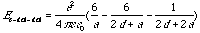
determine coupling effects between the two layers we convert the gate voltage
into an electron-energy (the electron energy in the dot measured from the GaAs
band edge) using the simplifying lever arm model given. e.g. in Refs. [2,3]
where 650 mV is the value for the Schottky barrier between the gate and the
GaAs cap. It is important to note that the lever arm for each of the two dot
layers is different (see Fig. 1): In our 20 nm-samples we have a lever arm of
1/7 for the first dot layer and 1/3.9 for the second one. Therefore the CV
spectra of a single layer sample with the same leverage than the second dot
layer would be compressed compared to the spectra of the first dot-layer alone.
In addition, as the gate voltage required to reach the charging threshold for
the dot scales linearily with the distance from the back contact to the dot
(t2 in Fig 1) it is also shifted to higher gate voltages. Fig. 3b
shows such a (calculated) spectrum. However, in the double layer sample we
expect the charging of the second dot layer to be influenced by
electron-electron interaction. In analogy to the Coulomb blockade within a dot
(which is responsible for the s and p-level splitting) we have in this case a
Coulomb blockade between dots of different layers. Using an electrostatical
approach this electron-electron interaction is modeled in the following way
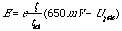
Ee-dot-dot is the additional Coulomb energy of an electron in dot 2
when dot 1 is filled with 6 electrons taking into account the image charges in
the back contact (s. inset of fig. 3). With d= 25 nm and a = 20 nm we obtain a
value of 24 meV. In addition, we take the next neighbours of dot A into
account. From an analysis of AFM data we estimate 4 next neighbours to be at
distances of 40 nm and thus the total Coulomb energy in this model adds up to
48 meV. The interaction with dots that are further apart laterally is
effectively screened out by the metallic back contact and can be neglected.
With the lever of 3.9 we would expect an energy shift of 0.19 V. Fig. 3c shows
the same trace as in Fig. 3b, but shifted by this additional inter-dot Coulomb
energy. As it matches very well with the 2 additional peaks in Fig. 3a, we
conclude that the additional peaks are indeed the s- and p-states of the second
dot layer and that the shift is a direct consequence of the dot-dot
interaction.
Magneto-capacitance on this sample confirms the energy diagrams, but as there
is no intermixing between the levels of the double-dot system (contrary to the
10 nm sample discussed later), the spectra correspond to those of two single
layer samples. It is to note that the energy level at Ug=0,85 V (labelled x in
Fig. 2a) is not yet understood. A possible scenario would be an additional
energy level in the wetting layer of the second dot system, created by the
strain field of the first dot-layer.
Fig. 4 shows the magneto-capacitance of the 10 nm sample. In contrast to the
20 nm sample deviations from the spectra of a single-layer sample already occur
within the charging of the p- shell. In this system the lever for the second
dot layer is 5 and the energy shift of 230 meV can again be explained quite
accurately using the model for electrostatic dot-dot interaction described
above. However, in this case the filling of the dots in the second layer will
add an additional Coulomb blockade term to the unfilled p-states of the first
dot layer. A sketch with energy levels that correspond to this situation is
shown in Fig. 5a. For B=0 charging of the second dot (s21) occurs
after the p-level of the first dot is filled with 3 electrons. The second
electron of dot 2 cannot be resolved, probabely due to charging of the
wettinglayer of dot 1. In single-layer samples the s-state is only little
affected by magnetic field, whereas the p-state shows characteristic Zeeman
splitting with two states increasing with increasing field and two decreasing
[7]. Applying this to the energy levels of the double-dot system we expect
p1 and p2 to decrease and p3 and p4
to increase with increasing magnetic field. When p3 reaches the
level of s21, the influence of the inter-dot Coulomb blockade
changes the charging sequence: For B=0 the p3 level of dot 1 will be
charged before the s21 level of the second dot, whereas at high
field, the s21 state will be charged first. Thus the combination of
orbital Zeemann splitting and Coulomb interaction between the dots results in a
magnetic-field-induced filling of the second s-state. This picture is confirmed
by Fig. 5b, which shows the difference between the magneto-capacitance of the
10 nm double-dot sample and a single-layer sample at various magnetic fields.
The development of the peaks shows that the cross-over takes place at
 6 T.
6 T.
In-plane dipole coupling within a single plane of dots was investigated on
single-layer samples. The FIR transmission of the sample shows absorption lines
corresponding to the allowed dipole dot-excitations [3] that are too narrow to
be explained by independent excitations in each dot of the ensemble. The
observed line width of 2-4 meV in these spectra is well below the broadening
that is related to size fluctuations, both in thickness and diameter of the
quantum dots. The energy difference E1-E0 (which is
measured in the FIR absorption) is predominantly affected by fluctuations of
the dot-dot diameter, whereas fluctuations of the dot thickness contribute
mainly to the ground state and thus broaden the charging threshold. AFM
investigations revealed fluctuations of the dot diameter of approx. 10 % [5].
Assuming a parabolic potential and

 50 meV, which is confirmed by earlier investigations [3], we therefore estimate
within a single -electron model a corresponding energy broadening of 10 meV. We
attribute the narrowing of the lines observed in the experiments to inter-dot
coupling effects. Then the FIR resonance can be seen as a collective response
of the dot ensemble as a whole. Such a collective mode can be expected whenever
the lateral coupling energy exceeds the energy broadening caused by size
fluctuations. Applying a model proposed by Merkt [8] we can
qualitativly explain this effect, but quantitative modelling of this system
requires elaborate numerical simulation and is beyond the purpose of this
paper.
50 meV, which is confirmed by earlier investigations [3], we therefore estimate
within a single -electron model a corresponding energy broadening of 10 meV. We
attribute the narrowing of the lines observed in the experiments to inter-dot
coupling effects. Then the FIR resonance can be seen as a collective response
of the dot ensemble as a whole. Such a collective mode can be expected whenever
the lateral coupling energy exceeds the energy broadening caused by size
fluctuations. Applying a model proposed by Merkt [8] we can
qualitativly explain this effect, but quantitative modelling of this system
requires elaborate numerical simulation and is beyond the purpose of this
paper.
We gratefully acknowledge financial support through BMBF grant 01BM623,
through the Max Planck Gesellschaft and through QUEST, a NSF Science and
Technology Center.
References
[1] L. Goldstein, F. Glas, J. Y. Marzin, M.N. Charasse, G. Le Roux,. Appl.
Phys. Lett 47, 1099 (1985); Q. Xie, A.. Madhukar, P. Chen, N.P.
Kobayashi. Phys. Rev. Lett. 75, 2542 (1995); M. Grundmann et al.
Phys. Rev. Lett. 74, 4043 (1995); J.-Y. Marzin, J.M. Gerard, A.
Izrael, D. Barrier, G. Bastard, Phys. Rev. Lett. 73, 716 (1994)
[2] H. Drexler, D. Leonard, W. Hansen, J.P. Kotthaus, P.M. Petroff,
Phys. Rev. Lett. 73 2252 (1994); G. Medeiros-Ribeiro, D.
Leonard, P.M. Petroff, Appl. Phys. Lett. 66, 1767 (1995)
[3] M. Fricke, A. Lorke, J.P. Kotthaus, G. Medeiros-Ribeiro, P.M. Petroff,
Europhys Lett. 36 197 (1996)
[4] S. Benjamin, N.F. Johnson, Appl. Phys. Lett. 70 2321
(1997)
[5] D. Leonard, M. Krishnamurthy, C.M. Reaves, S.P. Denbaars, P.M. Petroff,
Appl. Phys. Lett. 63 3203 (1993)
[6] J. Tersoff, C. Teichert, M.G. Lagally, Phys. Rev. Lett.
76, 1675 (1996)
[7] W. Hansen, T.P. Smith, K.Y. Lee, J.A. Brum, C.M. Knoedler, J.M Hong,
D.P. Kern, Phys. Rev. Lett. 62 2168 (1989)
[8] U. Merkt, Phys. Rev. Lett. 76 1134 (1996)
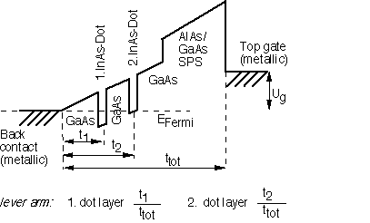
Fig. 1
Sketch of the conduction band edge of the investigated double-layer samples
with respect to the Fermi level Ef along the growth direction. The
indicated distances define the lever arm according to
ti/ttot which converts voltage differences into energy
differences. t1= 25 nm, t2 =45 nm (sample A) / 35 nm
(sample B), ttot =175 nm.
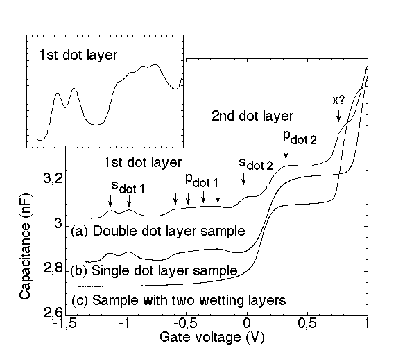
Fig. 2
Capacitance voltage (CV) traces of (a) a double-layer sample with vertically
stacked quantum dots at 20 nm distance (sample A); (b) a single-layer sample;
(c) a sample with two wetting layers The curves are offset for clarity. The
inset shows the charging of the first dot-layer of (a) at higher
magnification.
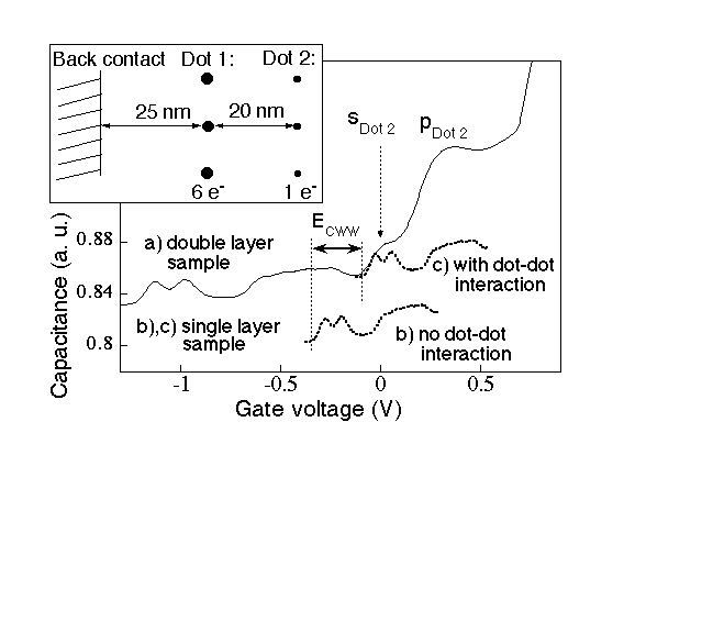
Fig. 3
(a) CV trace of 20 nm double dot sample; (b) calculated CV trace of a
single-dot sample with a lever arm corresponding to the second dot layer; (c)
CV spectra of (b) shifted in gate voltage by the calculated inter-dot layer
Coulomb energy. The inset shows schematically the applied electrostatic model
used for the calculation.
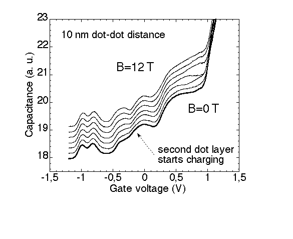
Fig. 4
Magnetocapacitance of a 10 nm double-dot sample (sample B) for magnetic fields
B=0,2,4,6,8,10,12 T. The curves are offset for clarity.
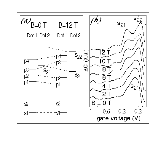
Fig. 5
(a)Schematic energy diagramm for the energy levels of dot 1 and dot 2 at B=0 T
and B=12 T; (b) Difference in capacitance between 10 nm double-dot sample and a
single-layer sample between B=0 T and B=12 T; the levels s21and
s22 correspond to the levels of the second dot in (a).