Experimental control of the number of ionized donors
in an AlGaAs/GaAs heterostructure
P. Denk, T. Schlösser, and K. Ensslin
Sektion Physik, LMU München, D-80539 München, Germany
M. Holland
Dept. of Electronics, University of Glasgow, United Kingdom
The high mobility of electrons in AlGaAs-GaAs heterostructures relies on the
concept of modulation doping. As a sample is cooled down to T=4.2 K under a
fixed gate bias the number of ionized donors can be frozen and is then
independent on the gate potential. We discuss the consequences of this
procedure on the electron density and mobility in a two-dimensional electron
gas. For a laterally patterned sample we find that the amplitude of the
potential modulation can be maximized for a given carrier density by a suitably
chosen cool down voltage.
PACS No: 73.20.Dx, 03.65.Sq, 73.50.Jt
The invention of modulation doping [1] has lead to the realization of
ultra-high electron mobilities in AlGaAs-GaAs heterostructures [2]. At low
temperatures the mobility is usually limited by Coulomb scattering of the
electrons at the residual impurities in the GaAs channel as well as at the
smooth potential perturbations arising from the ionized donors in the
intentionally doped region above the spacer layer. The electron density can be
calculated self-consistently [3] from the layer sequence and the number of
ionized donors which depends sensitively on the position of the Fermi energy at
room temperature. If the Fermi energy is changed at low temperatures the
thermal energy of the electrons is too low to overcome the AlGaAs barrier
between the electron channel and the doped region leading to a fixed degree of
ionization. The carrier density of the electrons, however, can still be tuned
with an external gate voltage at low temperatures because the number of ionized
donors is fixed. The method to cool down a sample under a fixed gate voltage
Vcd can therefore be used to realize different and fixed values of ionized
donors at low temperatures keeping all other sample parameters the same.
The possible correlation of ionized donors and the impact on the mobility of
the electron gas was investigated by Buks et al. [4]. Here we are rather
interested in the possibility to influence the potential and with it the
carrier density at a given gate voltage at low temperatures. In particular we
find that the number of ionized donors can be modified by a factor of two for
suitably chosen cool down voltages. Furthermore we show that the controlled
freezing of donors can be used to optimize the potential modulation of a
lateral superlattice.
The samples are grown by molecular beam epitaxy and have the following layer
sequence on top of the substrate and the buffer layer: 20 nm undoped AlxGa1-xAs
spacer, 12 nm Si doped AlxGa1-xAs, 13 nm undoped AlxGa1-xAs and 9 nm undoped
GaAs cap. The Al content is x = 0.3 and the doping level is 3x10¹⁸
cm-3 as calibrated on GaAs bulk samples. At T=4.2 K the carrier
density is 3.5x1011 cm-2 and the mobility 500 000
cm2/Vs. A gate electrode covering a Hall bar is evaporated enabling
us to apply a front gate voltage with respect to the two-dimensional electron
gas (2DEG).
At room temperature a finite gate voltage is applied and the sample is then
cooled down under this fixed cool-down voltage Vcd to a temperature of T =4.2
K. At this low temperature the magnetoresistance as well as the Hall resistance
is measured for different values of the gate voltage Vg in order to extract the
carrier density and the mobility. The experimentally obtained carrier density
as a function of gate voltage for several cool-down voltages is presented in
Fig. 1 (solid symbols). The four curves are parallel to each other indicating
the capacitor-like geometry between the front gate and the 2DEG. Above a
carrier density of Ns ~ 4.5 x 1011 cm-2 the curves
saturate. The additional electrons induced by the gate voltage start to occupy
states in the doped AlGaAs regions where the conduction band falls below the
Fermi energy. The arising parallel conduction of the sample can be detected in
the magnetoresistance.
In order to get a quantitative understanding of the change in the ionization
degree of the donors we solved Schrodinger and Poisson equation
self-consistently (see for example [3]) taking the layer thicknesses from the
growth as input parameters. The only free parameter in the calculation is the
number of ionized donors in the doped region. The open symbols in Fig. 1
represent results from this calculation for four values of ionized donor
concentrations as indicated in the inset (in units of 1018
cm-3). The general agreement with the experimental data is
excellent. The maximum number of ionized donors found from this analysis is 3.0
x 1018 cm-3 in close agreement with the value used in the
growth procedure. The minimum number is about half that value, namely 1.4 x
1018 cm-3. In that case only the shallow donors are
ionized representing about 50% of the total number of donors.
A superlattices of photoresist stripes is fabricated on the sample surface by
electron beam lithography and a suitable development and exposure process. The
pattern is transferred onto the 2DEG either by a carefully tuned wet etching
step [6] or by a gate voltage which is applied to a front gate electrode that
is evaporated on top of the patterned resist layer [7]. Both sample types lead
to qualitatively similar results and we will restrict ourselves in the
following to the discussion of the wet etched sample surface which was covered
with a gate electrode after the photoresist has been taken off.
For current flow perpendicular to the potential modulation commensurability
oscillations arise in the magnetoresistance [8] that can be used to extract the
amplitude of the potential modulation [9]. The effective potential modulation
in the plane of the 2DEG is found to be strongly reduced by screening effects.
[10] Figure 2 presents experimental data for the potential modulation as a
function of carrier density as tuned by a front gate voltage. The different
curves are obtained for different cool-down voltages Vcd.
For a sample surface patterned by wet etching the local carrier density is
reduced under etched areas. (see Fig. 3(a)) For a negative cool-down voltage
Vcd < 0 this leads to an enhanced and laterally more uniform density of
ionized donors under the etched areas. Since the distance between the sample
surface and the 2DEG is reduced in the etched areas any applied gate voltage
leads to a stronger electric field in those areas compared to the bare parts of
the sample surface and therefore to a further increase of the potential
modulation. (see Fig. 3(b)). This explains the increase in [[Delta]]Ns/Ns as
one goes from Vcd = 0 to Vcd = -300 mV in Fig. 2. For a further increase of the
negative cool-down voltage all donors will be ionized and the amplitude of the
potential modulation at a given value of Ns will then saturate (see Vcd=-300mV
to -500 mV in Fig. 2).
For positive cool-down voltages Vcd > 0 one obtains a small and laterally
uniform degree of ionization. In order to induce a given carrier density in the
channel one has to apply a very positive gate bias that acts especially strong
in the etched areas therefore compensating the original effect of the modulated
sample surface. The effective potential modulation does not depend very
strongly on the cool-down voltage (see Vcd=+300mV to +500 mV in Fig. 2,
schematically in Fig. 3(c)). At least qualitatively we can understand the
experimental observations as summarized in Fig. 2 by those straight forward
considerations. The laterally distributed ionized donors are able to enhance or
weaken the potential modulation depending on the sign of the cool-down voltage.
We therefore have a means to realize a desired amplitude of the potential
modulation by a well chosen cool-down voltage.
We are grateful to the Deutsche Forschungsgemeinschaft and the ESPRIT Basic
Research Action for financial support.
References
[1] H. L. Störmer, A. C. Gossard, and W. Wiegmann, Solid State
Commun. 41, 707 (1982)
[2] L. N. Pfeiffer, K. W. West, H. L. Störmer, and K. Baldwin, Appl. Phys.
Lett. 55, 1888 (1989)
[3] F. Stern and S. Das Sarma, Phys. Rev. B30, 840 (1984)
[4] E. Buks, M. Heiblum, Y. Levinson, and H. Shtrikman, Semicond. Sci. Technol.
9, 2031 (1994)
[5] K. Hirakawa and H. Sakaki, Phys. Rev. B33, 8291 (1986)
[6] R. Schuster, K. Ensslin, D. Wharam, S. Kühn, J. P. Kotthaus, G.
Böhm, W. Klein, G. Tränkle, and G. Weimann, Phys. Rev. B49,
8510 (1994)
[7] T. Schlösser, K. Ensslin, F. Claro, J. P. Kotthaus, M. Holland, and R.
Ketzmerick, Phys. Rev. B April 15 1995
[8] D. Weiss, K. v. Klitzing, K. Ploog, and G. Weimann, Europhys. Lett.
8, 179 (1989)
[9] A. K. Geim, R. Taboryski, A. Kristensen, S. V. Dubonos, and P. E. Lindelof,
Phys. Rev. B46, 4324 (1992)
[10] J. P. Kotthaus and D. Heitmann, Surf. Science 113, 481 (1982)
Figure Captions
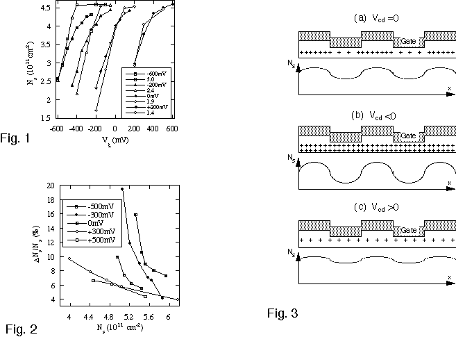
Fig. 1: Carrier density as extracted from low temperature Shubnikov-de
Haas oscillations as a function of gate voltage for a laterally homogeneous
AlGaAs/GaAs heterostructure. The parameter in the experimental curves (solid
symbols) is the cool-down voltage. The open symbols are obtained from a
self-consistent calculation and the corresponding parameter is the density of
ionized donors.
Fig. 2: Effective lateral modulation of the carrier density extracted from a
theoretical analysis of commensurability oscillations as a function of
normalized carrier density for a laterally patterned electron gas.
Fig. 3: Schematic of the sample structure for several cool-down voltages. The
layer of crosses indicates the position of the ionized donors, the hatched area
on top represents the gate metal and the amplitude of the Ns versus x curves
gives an estimate for the effective potential modulation.